5 commands, 6 interrupt request register (al event register), 7 write access – BECKHOFF EtherCAT IP Core for Xilinx FPGAs v2.04e User Manual
Page 95: 8 read access, Commands, Interrupt request register (al event register), Write access, Read access, Table 45: spi commands cmd0 and cmd1, Table 46: interrupt request register transmission
PDI Description
Slave Controller
– IP Core for Xilinx FPGAs
III-83
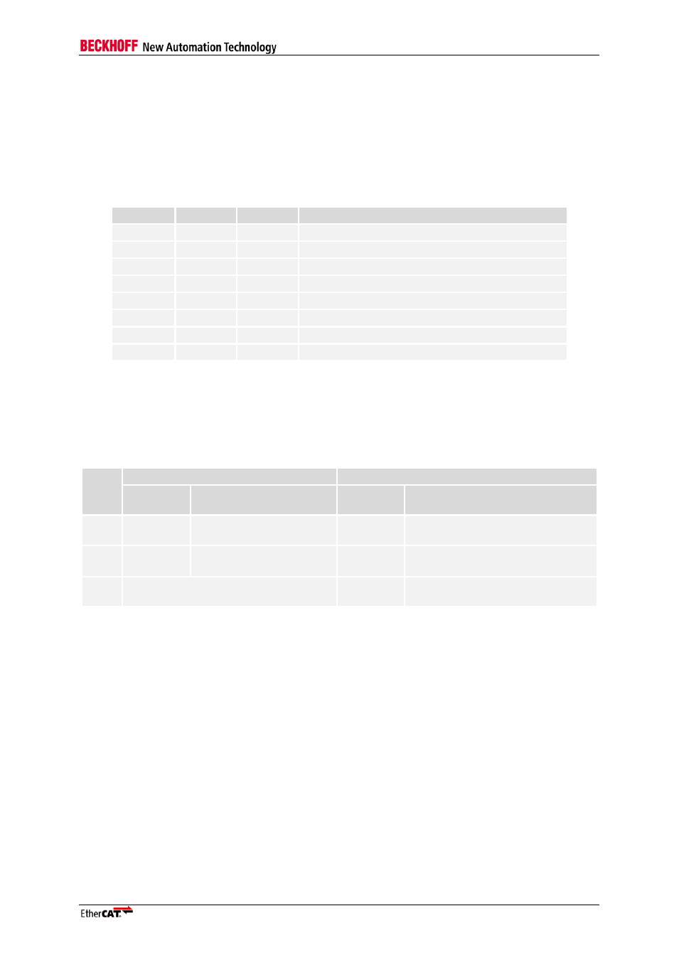
10.2.5 Commands
The command CMD0 in the second address/command byte may be READ, READ with following Wait
State bytes, WRITE, NOP, or Address Extension. The command CMD1 in the third address/command
byte may have the same values:
Table 45: SPI commands CMD0 and CMD1
CMD[2]
CMD[1]
CMD[0]
Command
0
0
0
NOP (no operation)
0
0
1
reserved
0
1
0
Read
0
1
1
Read with following Wait State bytes
1
0
0
Write
1
0
1
reserved
1
1
0
Address Extension (3 address/command bytes)
1
1
1
reserved
10.2.6 Interrupt request register (AL Event register)
During the address phase, the SPI slave transmits the PDI interrupt request registers 0x0220-0x0221
(2 byte address mode), and additionally register 0x0222 for 3 byte addressing on SPI_DO (MISO):
Table 46: Interrupt request register transmission
Byte
2 Byte address mode
3 Byte address mode
SPI_DI
(MOSI)
SPI_DO
(MISO)
SPI_DI
(MOSI)
SPI_DO
(MISO)
0
A[12:5]
I0[7:0]
interrupt request
register 0x0220
A[12:5]
I0[7:0]
interrupt request register
0x0220
1
A[4:0]
CMD0[2:0]
I1[7:0]
interrupt request
register 0x0221
A[4:0]
CMD0[2:0]
I1[7:0]
interrupt request register
0x0221
2
(Data phase)
A[15:13]
CMD1[2:0]
I2[7:0]
interrupt request register
0x0222
10.2.7 Write access
In the data phase of a write access, the SPI master sends the write data bytes to the SPI slave
(SPI_DI/MOSI). The write access is terminated by taking back SPI_SEL after the last byte. The
SPI_DO signal (MISO) is undetermined during the data phase of write accesses.
10.2.8 Read access
In the data phase of a read access, the SPI slave sends the read data bytes to the SPI master
(SPI_DO/MISO).