9 timing specification, Timing specification – BECKHOFF EtherCAT IP Core for Xilinx FPGAs v2.04e User Manual
Page 108
PDI Description
III-96
Slave Controller
– IP Core for Xilinx FPGAs
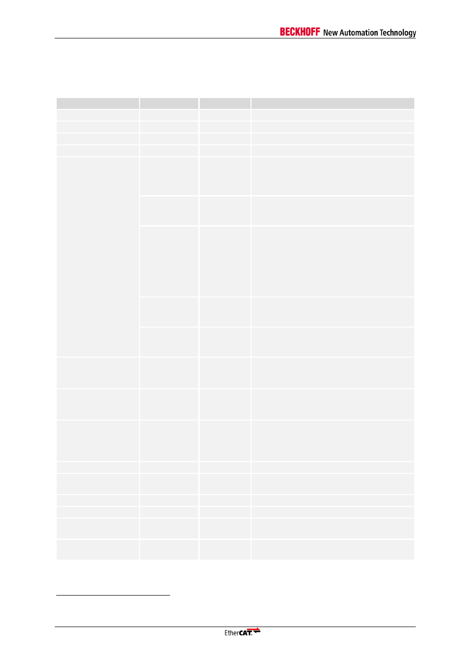
10.3.9 Timing Specification
Table 53: µController timing characteristics IP Core
Parameter
Min
Max
Comment
t
CS_to_BUSY
x
10
BUSY driven and valid after CS assertion
t
ADR_BHE_setup
ADR and BHE valid before RD assertion
t
RD_to_DATA_driven
0 ns
11
DATA bus driven after RD assertion
t
RD_to_BUSY
BUSY asserted after RD assertion
t
read
External read time (RD assertion to BUSY
deassertion) with normal read busy output
(0x0152[0]). Additional 20 ns if delayed read
busy output is configured.
a) t
read_int
a) without preceding write access or
t
WR_to_RD
≥
t
prec_write
+ t
Coll
or configuration:
write after falling edge of WR
b) t
read_int
+ t
prec_write
+t
Coll
-t
b) with preceding write access and
t
WR_to_RD
< t
prec_write
+ t
Coll
c) 420 ns
c) 8 bit access, absolute worst case with
preceding write access (t
WR_to_RD
=min
,
t
prec_write
=max, t
Coll
=max)
d) 560 ns
d) 16 bit access, absolute worst case with
preceding write access (t
WR_to_RD
=min
,
t
prec_write
=max, t
Coll
=max)
t
read_int
a) 220 ns
b) 300 ns
Internal read time
a) 8 bit access
b) 16 bit access
t
prec_write
a) 180 ns
b) 260 ns
Time for preceding write access
a) 8 bit access
b) 16 bit access
t
BUSY_to_DATA_valid
-5 ns
-20 ns
DATA bus valid after device BUSY is
deasserted
a) normal read busy output
b) delayed read busy output
t
ADR_BHE_to_DATA_invalid
DATA invalid after ADR or BHE change
t
CS_RD_to_DATA_release
DATA bus released after CS deassertion or
RD deassertion
t
CS_to_BUSY_release
BUSY released after CS deassertion
t
CS_delay
Delay between CS deassertion an assertion
t
RD_delay
Delay between RD deassertion and
assertion
t
ADR_BHE_DATA_setup
ADR, BHE and Write DATA valid before WR
deassertion
10
EtherCAT IP Core: time depends on synthesis results
11
EtherCAT IP Core: time depends on synthesis results, specified value has to be met anyway