8 ip core signals, 1 general signals, 1 clock source example schematics – BECKHOFF EtherCAT IP Core for Xilinx FPGAs v2.04e User Manual
Page 65: Ip core signals, General signals, Clock source example schematics, Table 18: general signals, Figure 24: ethercat ip core clock source (mii)
IP Core Signals
Slave Controller
– IP Core for Xilinx FPGAs
III-53
8
IP Core Signals
The available signals depend on the IP Core configuration.
8.1
General Signals
Table 18: General Signals
Condition
Name
Direction
Description
nRESET
INPUT
Resets all registers of the
IP Core, active low
Reset slave by
ECAT/PDI
RESET_OUT
OUTPUT
Reset by ECAT (reset
register 0x0040), active
high. RESET_OUT has to
trigger nRESET, which
clears RESET_OUT.
CLK25
INPUT
25 MHz clock signal from
PLL (rising edge
synchronous with rising
edge of CLK100)
CLK100
INPUT
100 MHz clock signal from
PLL
8.1.1
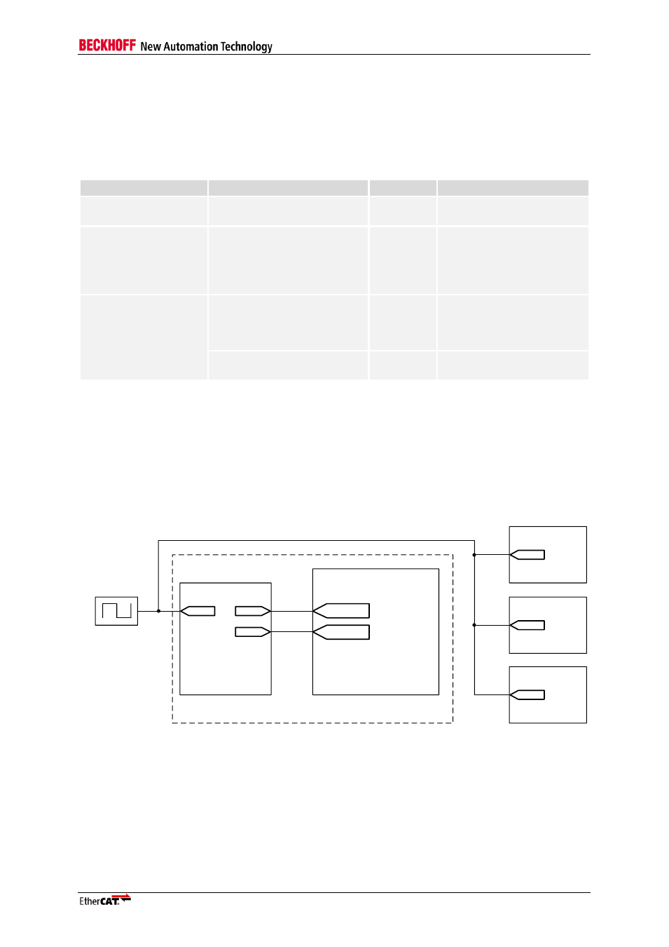
Clock source example schematics
The EtherCAT IP Core and the Ethernet PHYs have to share the same clock source. The initial
accuracy of the EtherCAT IP clock source has to be 25ppm or better.
Typically, the clock inputs of the EtherCAT IP Core (CLK25, CLK100, and optionally CLK50) are
sourced by a DCM/PLL inside the FPGA. The DCM/PLL has to use a configuration which guarantees
a fixed phase relation between clock input and clock outputs, in order to enable TX shift compensation
for the MII TX signals.
CLK25
EtherCAT IP Core
Ethernet
PHY
MII
CLK25
DCM/PLL
CLK_IN
CLK25
CLK100
CLK100
Ethernet
PHY
MII
CLK25
25 MHz
Ethernet
PHY
MII
CLK25
FPGA
Figure 24: EtherCAT IP Core clock source (MII)