2 tx shift compensation, Tx shift compensation, Figure 29: mii tx timing diagram – BECKHOFF EtherCAT IP Core for Xilinx FPGAs v2.04e User Manual
Page 82
Ethernet Interface
III-70
Slave Controller
– IP Core for Xilinx FPGAs
9.2.2
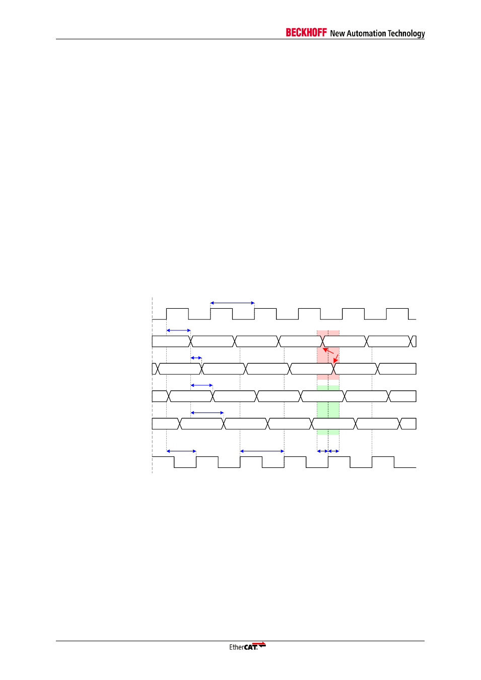
TX Shift Compensation
Since IP Core and the Ethernet PHYs share the same clock source, TX_CLK from the PHY has a
fixed phase relation to MII_TX_ENA/MII_TX_DATA from the IP Core. Thus, TX_CLK is not connected
and the delay of a TX FIFO inside the IP Core is saved.
In order to fulfill the setup/hold requirements of the PHY, the phase shift between TX_CLK and
MII_TX_ENA/MII_TX_DATA has to be controlled. There are several alternatives:
TX Shift Compensation by specifying/verifying minimum and maximum clock-to-output times for
MII_TX_ENA/MII_TX_DATA with respect to CLK_IN (PHY and PLL clock source).
TX Shift compensation with additional delays for MII_TX_ENA/MII_TX_DATA of 10, 20, or 30 ns.
Such delays can be added using the TX Shift feature and applying MII_TX_SHIFT[1:0].
MII_TX_SHIFT[1:0] determine the delay in multiples of 10 ns for each port. For guaranteed
timings, maximum clock-to-output times for MII_TX_ENA/MII_TX_DATA should be applied, too.
Set MII_TX_CLK to 0 if manual TX Shift compensation is used.
Automatic TX Shift compensation if the TX Shift feature is selected: connect MII_TX_CLK and the
automatic TX Shift compensation will determine correct shift settings. For guaranteed timings,
maximum clock-to-output times for MII_TX_ENA/MII_TX_DATA should be applied, too. Set
manual TX Shift compensation to 0 in this case.
MII_TX_ENA and MII_TX_DATA are generated synchronous to CLK25, although the source registers
are both CLK25 and CLK100 registers.
The PLL/DCM has to use a configuration which guarantees a fixed phase relation between clock input
and CLK25/CLK100 output, in order to enable TX shift compensation for the MII TX signals.
CLK_IN
TX_CLK
MII_TX_ENA
MII_TX_DATA
MII_TX_ENA
MII_TX_DATA
MII_TX_ENA
MII_TX_DATA
MII_TX_ENA
MII_TX_DATA
MII_TX_ENA
MII_TX_DATA
MII_TX_ENA
MII_TX_DATA
MII_TX_ENA
MII_TX_DATA
MII_TX_ENA
MII_TX_DATA
MII_TX_ENA
MII_TX_DATA
MII_TX_ENA
MII_TX_DATA
MII_TX_ENA
MII_TX_DATA
MII_TX_ENA
MII_TX_DATA
MII_TX_ENA
MII_TX_DATA
MII_TX_ENA
MII_TX_DATA
MII_TX_ENA
MII_TX_DATA
MII_TX_ENA
MII_TX_DATA
t
CLK25
10 ns
20 ns
30 ns
t
TX_delay
t
PHY_TX_hold
t
PHY_TX_setup
Wrong: Setup/Hold Timing violated
Good: Setup/Hold Timing met
t
CLK25
t
PHY_TX_CLK
MII_TX_ENA, MII_TX_DATA
MII_TX_ENA, MII_TX_DATA
+10 ns additional delay
MII_TX_ENA, MII_TX_DATA
+20 ns additional delay
MII_TX_ENA, MII_TX_DATA
+30 ns additional delay
Figure 29: MII TX Timing Diagram