3 mii timing specifications, Mii timing specifications, Table 36: mii tx timing characteristics – BECKHOFF EtherCAT IP Core for Xilinx FPGAs v2.04e User Manual
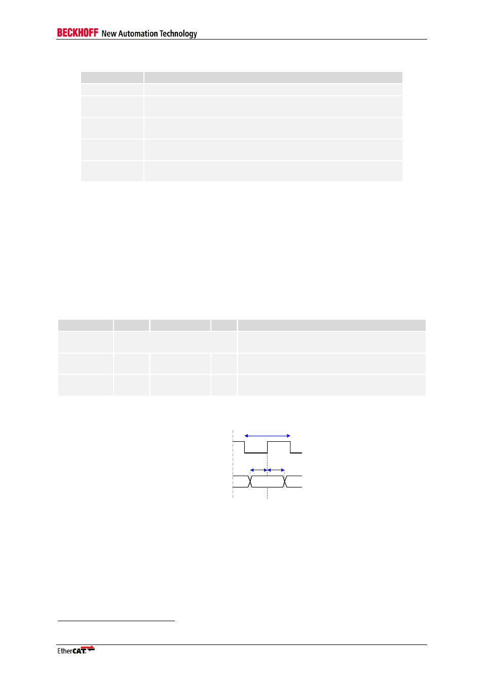
Page 83: Table 37: mii timing characteristics, Figure 30: mii timing rx signals

Ethernet Interface
Slave Controller
– IP Core for Xilinx FPGAs
III-71
Table 36: MII TX Timing characteristics
Parameter
Comment
t
CLK25
25 MHz quartz oscillator (CLK_IN)
t
TX_delay
MII_TX_ENA/MII_TX_DATA[3:0] delay after rising edge of CLK_IN,
depends on synthesis results
t
PHY_TX_CLK
Delay between PHY clock source and TX_CLK output of the PHY,
PHY dependent
t
PHY_TX_setup
PHY setup requirement: TX_ENA/TX_DATA with respect to TX_CLK
(PHY dependent, IEEE802.3 limit is 15 ns)
t
PHY_TX_hold
PHY hold requirement: TX_ENA/TX_DATA with respect to TX_CLK
(PHY dependent, IEEE802.3 limit is 0 ns)
If the phase shift between CLK25 and TX_CLK should not be constant for a some special PHYs,
additional FIFOs for MII_TX_ENA/MII_TX_DATA are necessary. The FIFO input uses CLK25, the
FIFO output TX_CLK[0] or TX_CLK[1] respectively.
NOTE: The phase shift can be adjusted by displaying TX_CLK of a PHY and MII_TX_ENA/MII_TX_DATA[3:0] on
an oscilloscope. MII_TX_ENA/MII_TX_DATA[3:0] is allowed to change between 0 ns and 25 ns after a rising
edge of TX_CLK (according to IEEE802.3
– check your PHY’s documentation). Setup phase shift so that
MII_TX_ENA/MII_TX_DATA[3:0] change near the middle of this range. MII_TX_ENA/MII_TX_DATA[3:0] signals
are generated at the same time.
9.2.3
MII Timing specifications
Table 37: MII timing characteristics
Parameter
Min
Typ
Max
Comment
t
RX_CLK
40 ns ± 100 ppm
RX_CLK period (100 ppm with maximum FIFO
Size only)
t
RX_setup
x
3
RX_DV/RX_DATA/RX_D[3:0] valid before rising
edge of RX_CLK
t
RX_hold
RX_DV/RX_DATA/RX_D[3:0] valid after rising
edge of RX_CLK
RX_DV
RX_D[3:0]
RX_ERR
RX_CLK
t
RX_setup
t
RX_hold
RX signals valid
t
RX_CLK
Figure 30: MII timing RX signals
3
EtherCAT IP Core: time depends on synthesis results
