3 p2 connector, Table 3-6, P2 connector pinout – Artesyn iVPX7225 Installation and Use (April 2015) User Manual
Page 63: Controls, leds and connectors
Controls, LEDs and Connectors
iVPX7225 Installation and Use (6806800S11C)
44
3.4.3
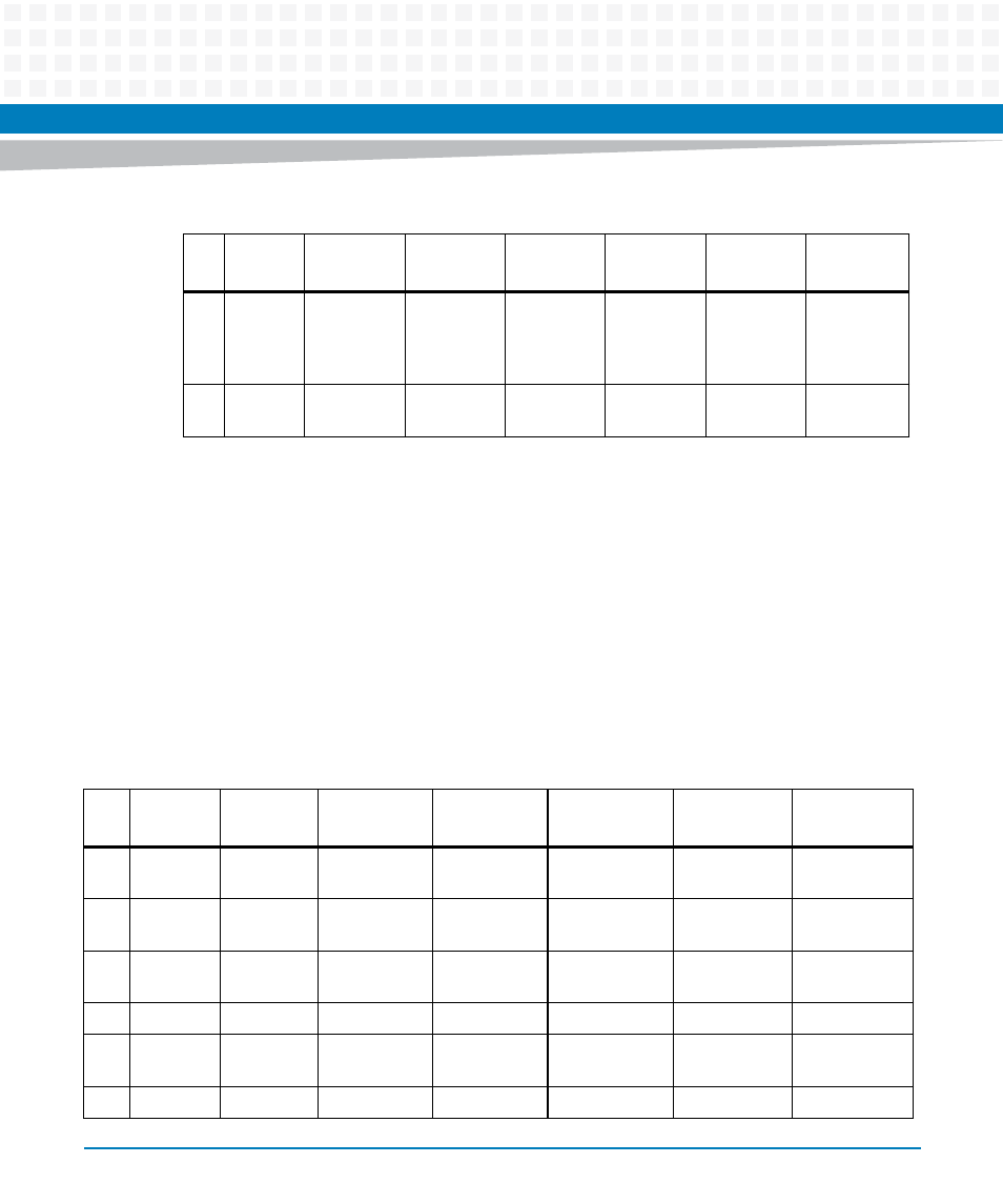
P2 Connector
The following table provides the pinout of the P2 connector.
15
MRST L
(4.75K PU
to 3.3V
AUX VPX)
GND
ETH LANE 1
TX N
ETH LANE 1
TX P
GND
ETH LANE 1
RX N
ETH LANE 1
RX P
16
GND
ETH LANE 0
TX N
ETH LANE 0
TX P
GND
ETH LANE 0
RX N
ETH LANE 0
RX P
GND
1. The iVPX7225 PCH supports a battery-backed real-time clock with 256 bytes of battery-backed RAM. The PCH
maintains the time of the day and stores system data as long as the VBAT input remains above 2V (at the iVPX7225
PCH RTC input). In the event that the, system does not provide a voltage at VBAT, there is a diode protected 0.2F
SuperCap (C214) onboard the iVPX7225 RTM to maintain operation for short down times. The steady state current
draw from the iVPX7225 at VBAT is 6 uA. In the event that VBAT is connected to 3.3V_AUX at the backplane, the RTM
SuperCap will discharge more quickly when 3.3V_AUX is removed. This is due to (SYSRESET) terminations present on
the VPX backplane. This could result in the loss of RTC and/or system data stored in the iVPX7225 PCH battery-
backed RAM. Refer to VITA 46 for additional information on the VBAT bussed signal.
Table 3-5 P1 Connector Pinout (continued)
Pin Row G
Row F
Row E
Row D
Row C
Row B
Row A
Table 3-6 P2 Connector Pinout
Pin
Row G
Row F
Row E
Row D
Row C
Row B
Row A
1
SPI WP OR L GND
COM0 RX CTS
N
COM0 RX
GND
COM0 RTS
COM0 TX
2
GND
COM1 RTS
TX N
COM1 RTS TX P GND
COM1 RX CTS N COM1 RX CTS P GND
3
IPMI WP OR
L
GND
ETH WP OR L
PCIE SW WP OR GND
IPMC DEBUG
RXD
IPMC DEBUG
TXD
4
GND
RTM TX DIS VPD WP OR L
GND
SMB CLK
SMB DATA
GND
5
NAND WP
OR L
GND
SATA P0 TX N
SATA P0 TX P
GND
SATA P0 RX N
SATA P0 RX P
6
GND
SATA P1 TX N SATA P1 TX P
GND
SATA P1 RX N
SATA P1 RX P
GND