Table 7-41, Logical device common decode ranges, Table 7-39 – Artesyn iVPX7225 Installation and Use (April 2015) User Manual
Page 145: Logical device base io address msb register, Table 7-40, Logical device base io address lsb register, Fpga registers
FPGA Registers
iVPX7225 Installation and Use (6806800S11C)
126
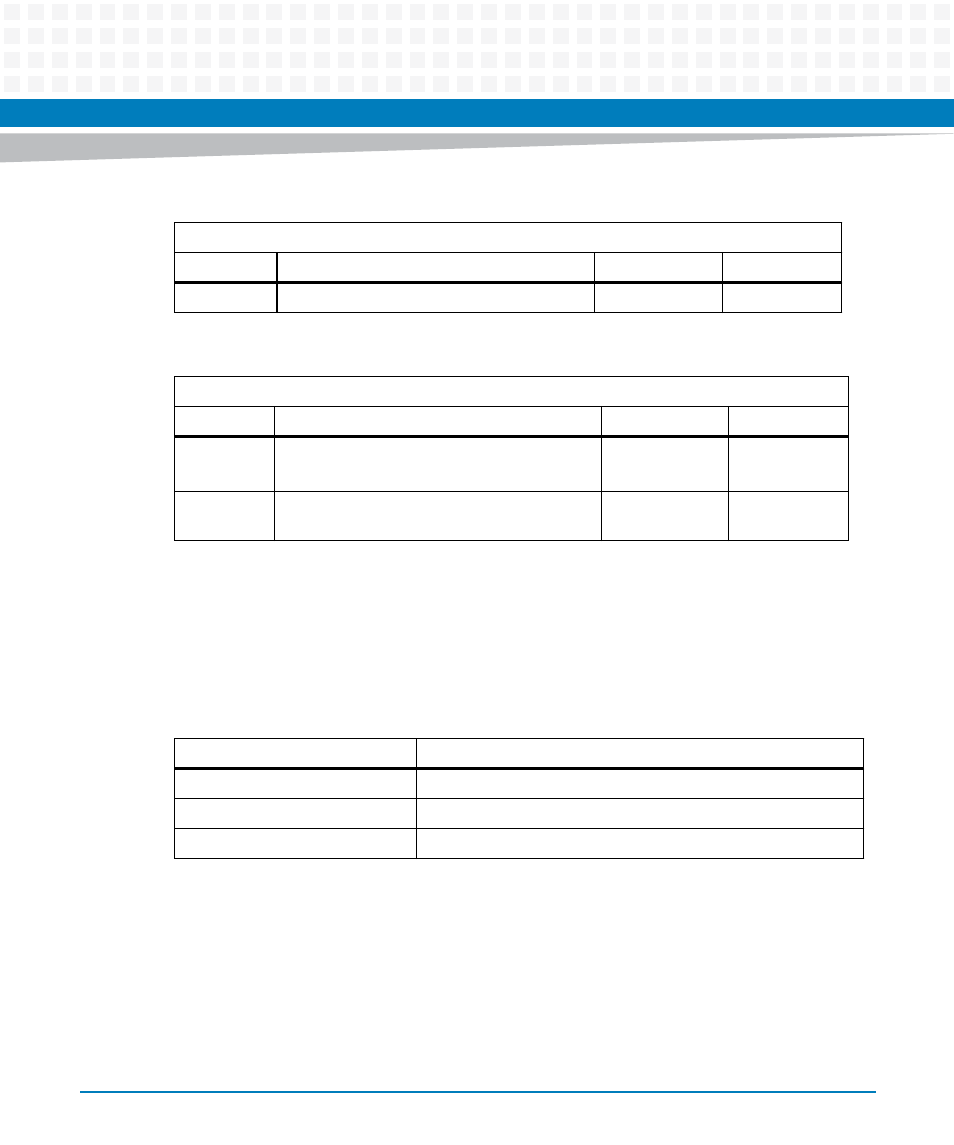
Registers 0x60 (MSB) and 0x61 (LSB) set the Logical Device Base IO for this logical device. For
example for Base IO address 0x3F8 the content of Register 0x60 is 0x03 and the content of
Register 0x61is 0xF8.
See table below for default IO addresses:
Table 7-39 Logical Device Base IO Address MSB Register
Index Address: 0x60
Bit #
Description
Default
Access
7:0
Logical Device Base IO Address MSB
0
LPC: R/W
Table 7-40 Logical Device Base IO Address LSB Register
Index Address: 0x61
Bit #
Description
Default
Access
2:0
Bits 0 to 2 are read only. Decode is on 8 Byte
boundary.
0
LPC: R
7:3
Logical Device Base IO Address LSB. (Bits 3 to
7)
0
LPC: R/W
Table 7-41 Logical Device Common Decode Ranges
IO Address range
Description
0x3F8 – 0x3FF
COM1
0x2F8 – 0x2FF
COM2
0x2E8 – 0x2EF
COM3
- ARTM-9405 16x10GbE Installation and Use Guide (May 2014) (64 pages)
- ATCA 7370 / ATCA 7370-S Installation and Use (January 2015) (256 pages)
- ATCA 7370 / ATCA 7370-S Installation and Use (September 2014) (254 pages)
- ARTM-831X Installation and Use (June 2014) (346 pages)
- ATCA-7350 - Integrating with Workbench User Guide (September 2014) (34 pages)
- ATCA-7350 Installation and Use (September 2014) (208 pages)
- ATCA-7365-CE Installation and Use (May 2014) (306 pages)
- ATCA-7365-CE Installation and Use (Jan 2015) (300 pages)
- ATCA-7365-CE Installation and Use (May 2014) (294 pages)
- ATCA-7368 Installation and Use (June 2014) (222 pages)
- ATCA-7475 Installation and Use (October 2014) (284 pages)
- ATCA-7480 Installation and Use (April 2015) (330 pages)
- ATCA-8330 Installation and Use (April 2015) (236 pages)
- ATCA-8320 Installation and Use (May 2014) (456 pages)
- ATCA-9305 User's Manual (May 2014) (270 pages)
- ATCA-9405 Installation and Use (October 2014) (168 pages)
- ATCA-F120 Installation and Use (August 2014) (122 pages)
- ATCA-F140 Installation and Use (September 2014) (138 pages)
- ATCA-MF106 Installation and Use (September 2014) (86 pages)
- Centellis-4440/AXP1440 Installation and Use (September 2014) (208 pages)
- Centellis 4410 (AXP-1410) Installation and Use (July 2014) (202 pages)
- Centellis 2100 Release 3.0 Installation and Use (March 2015) (192 pages)
- Centellis 2100 Release 3.0 Installation and Use (March 2015) (176 pages)
- Centellis 2000 User Card-10GE Installation and Use (May 2014) (54 pages)
- Centellis 2000 User Card-10GE with Telco Alarm Installation and Use (May 2014) (60 pages)
- COMX-CAR-210 Installation and Use (August 2014) (76 pages)
- COMX-P1022 Installation and Use (July 2014) (84 pages)
- COMX-P2020 Installation and Use (February 2015) (100 pages)
- COMX-CORE Series Installation and Use (August 2014) (128 pages)
- COMX-P2020 Installation and Use (July 2014) (100 pages)
- COMX-P4080-2G-ENP2 Installation and Use (August 2014) (70 pages)
- COMX-P4080 Installation and Use (August 2014) (126 pages)
- COMX-P40x0 ENP2 Installation and Use (August 2014) (130 pages)
- COMX-P40x0 ENP2 Installation and Use (January 2015) (140 pages)
- iVPX7225 RTM Installation and Use (April 2015) (56 pages)
- MITX-430/MITX-440-DVI-2E Installation and Use (August 2014) (118 pages)
- CPCI-6200 Installation and Use (May 2015) (234 pages)
- SCP-MITX-CORE-820-SM Installation and Use (August 2014) (132 pages)
- MVME2502 Installation and Use (December 2014) (166 pages)
- MVME2502 Installation and Use (August 2014) (150 pages)
- MVME2500 VxWorks 6.8 AMP User Guide (August 2014) (40 pages)
- MVME2500 VxWorks 6.8 User Guide (April 2014) (44 pages)
- MVME3100 Single Board Computer Installation and Use (June 2014) (156 pages)
- MVME4100 Single Board Computer Installation and Use (June 2014) (136 pages)