Table 7-53, Line status register (lsr), Fpga registers – Artesyn iVPX7225 Installation and Use (April 2015) User Manual
Page 157
FPGA Registers
iVPX7225 Installation and Use (6806800S11C)
138
Bits one through four are the error conditions that produce a receiver line status interrupt when
any of the corresponding conditions are detected and the interrupt is enabled. These bits are
not cleared by reading the erroneous byte from the FIFO or receive buffer. They are cleared only
by reading LSR. In FIFO mode, the line status interrupt occurs only when the erroneous byte is
at the top of the FIFO. If the erroneous byte being received is not at the top of the FIFO, an
interrupt is generated only after the previous bytes are read and the erroneous byte is moved
to the top of the FIFO.
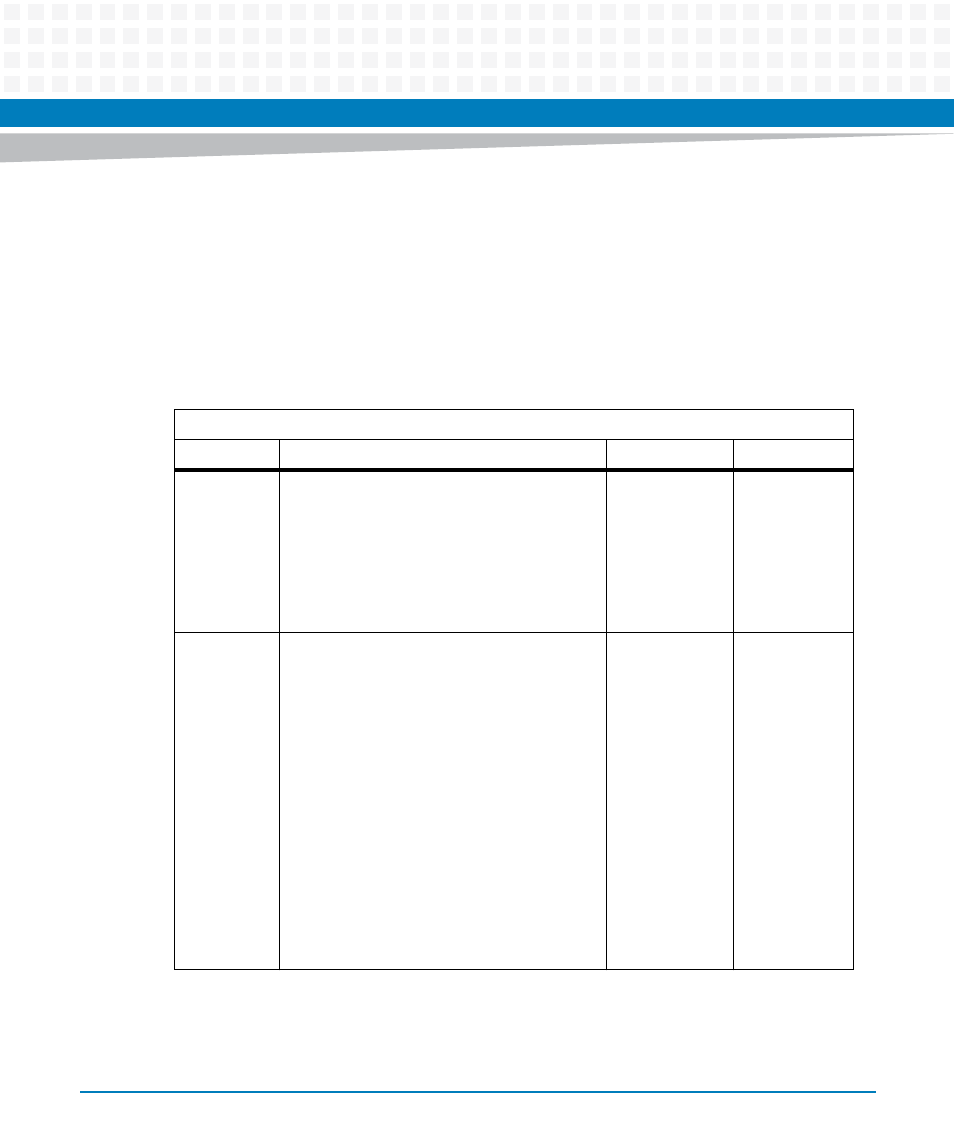
Table 7-53 Line Status Register (LSR)
IO Address: Base +5
Bit #
Description
Default
Access
0
Receiver data ready (DR) indicator
DR is set whenever a complete incoming
character has been received and transferred
into the RBR or the FIFO. DR is cleared by
reading all of the data in the RBR or the FIFO:
1: New data received
0: No new data
0
R
1
Overrun error (OE) indicator
When OE is set, it indicates that before the
character in the RBR was read, it was
overwritten by the next character transferred
into the register. OE is cleared every time the
CPU reads the contents of the LSR. If the FIFO
mode data continues to fill the FIFO beyond
the trigger level, an overrun error occurs only
after the FIFO is full and the next character has
been completely received in the shift register.
An overrun error is indicated to the CPU as
soon as it happens. The character in the shift
register is overwritten but it is not transferred
to the FIFO:
1: Overrun error occurred
0: No overrun error
0
R