6 logical device configuration registers, Table 7-37, Logical device configuration register summary – Artesyn iVPX7225 Installation and Use (April 2015) User Manual
Page 144: Table 7-38, Logical device enable register, Fpga registers
FPGA Registers
iVPX7225 Installation and Use (6806800S11C)
125
7.2.1.6
Logical Device Configuration Registers
Use to access the registers that are assigned to each logical device. The Super IO supports three
logical units and has three sets of logical device registers. The two logical devices are UART 1
(Logical Number 4), UART 2(Logical Number 5) and UART 3(Logical Number 6). A separate set
(bank) of control and configuration registers exists for each logical device and is selected with
the Logical Device Number Register. The INDEX PORT is used to select a specific logical device
register. These registers are then accessed through the DATA PORT. The Logical Device
registers are accessible only when the SIO is in the Configuration state.
The logical register addresses are shown in the tables below.
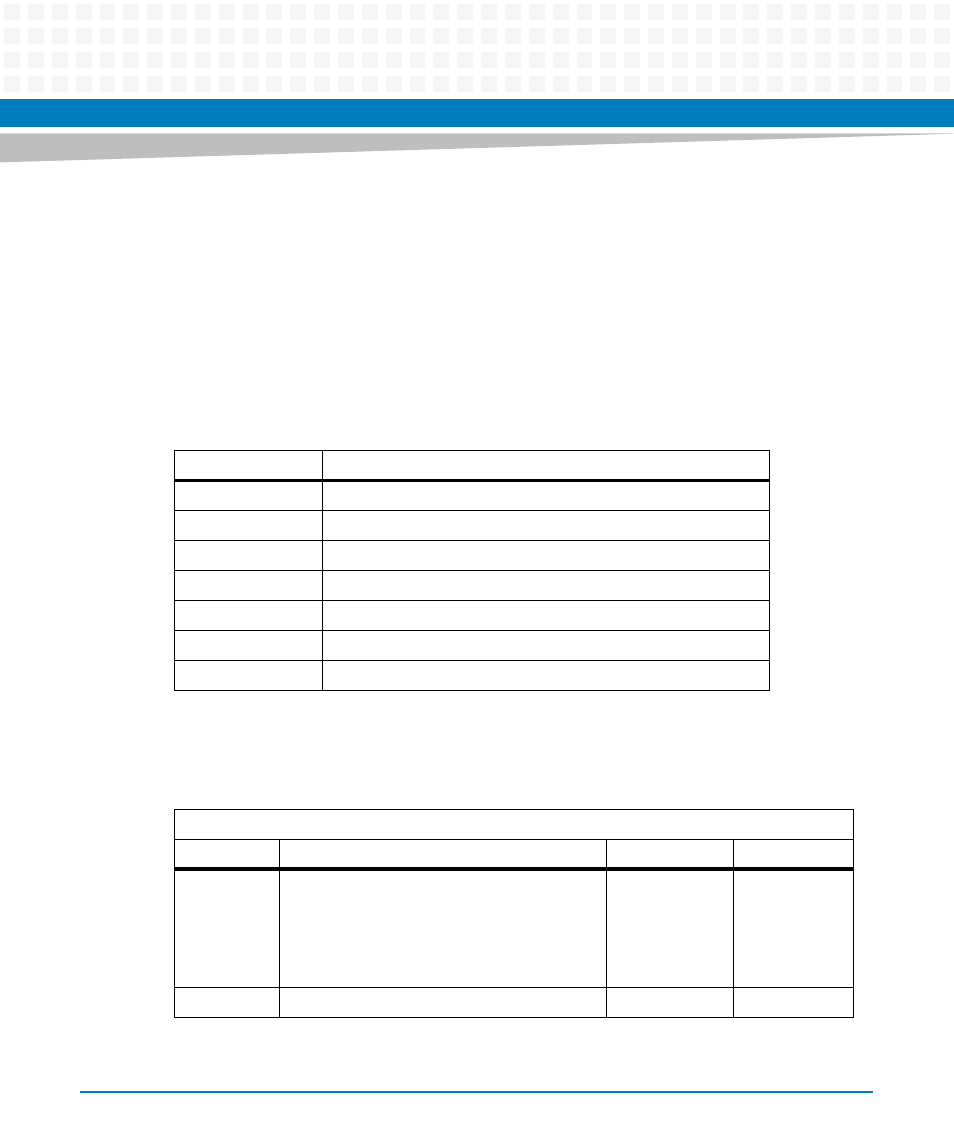
Table 7-37 Logical Device Configuration Register Summary
Index Address
Description
0x30
Enable
0x60
Base IO Address MSB
0x61
Base IO Address LSB
0x70
Primary Interrupt Select
0x74
Reserved
0x75
Reserved
0xF0
Reserved
Table 7-38 Logical Device Enable Register
Index Address: 0x30
Bit #
Description
Default
Access
0
Logical Device Enable:
0: disabled. Currently selected device is
inactive.
1: enabled. The currently selected device is
enabled.
1
LPC: R/W
7:1
Reserved
0
LPC: R