3 uart register overview, 1 uart registers dlab=0, Table 7-43 – Artesyn iVPX7225 Installation and Use (April 2015) User Manual
Page 147: Uart register overview, Fpga registers
FPGA Registers
iVPX7225 Installation and Use (6806800S11C)
128
7.3
UART Register Overview
The UART units may be mapped via Super IO (LPC bus).
shows the registers and their addresses as offsets of a base address for one of the
two UART units.
The state of the Divisor Latch Bit (DLAB), which is the MOST significant bit of the Serial Line
Control Register (SCR), affects the selection of certain of the UART registers. The DLAB bit must
be set high by the system software to access the Baud Rate Generator Divisor Latches (DLL and
DLM).
7.3.1
UART Registers DLAB=0
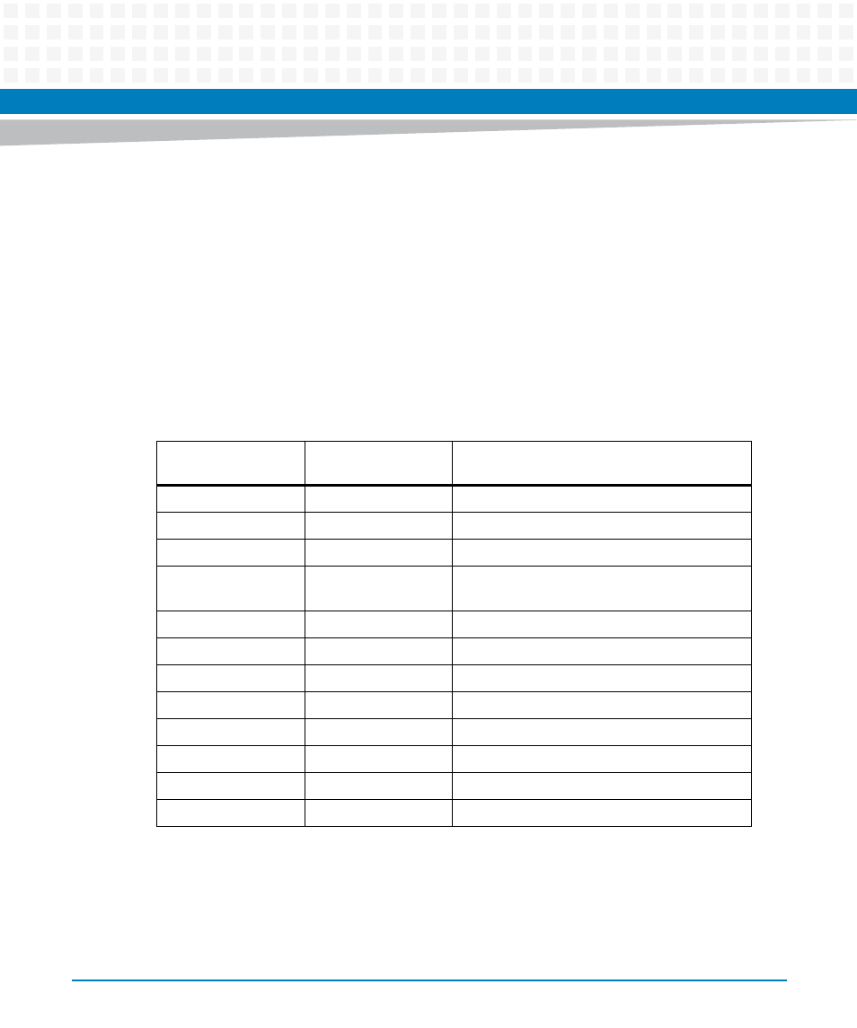
Table 7-43 UART Register Overview
LPC IO or Primary I/O
Address
DLAB Bit value
Description
Base
0
Receiver Buffer (RBR). Read Only.
Base
0
Transmitter Holding (THR). Write Only.
Base + 1
0
Interrupt Enable Register (IER)
Base + 2
X
Interrupt Identification Register (IIR). Read
Only.
Base + 2
X
FIFO Control Register (FCR). Write Only.
Base + 3
X
Line Control Register (LCR)
Base + 4
X
Modem Control Register (MCR)
Base + 5
X
Line Status Register (LCR). Read Only.
Base + 6
X
Modem Status Register. Read Only.
Base + 7
X
Scratch Pad Register (SCR)
Base
1
Division Latch LSB (DLL)
Base + 1
1
Division Latch MSB (DLM)