Elecraft XV Assembly Manual for XV222 User Manual
Page 54
- 51 -
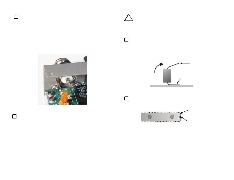
Connect J1 to the leads already soldered to the RF PCB as follows (See
Figure 41):
_ Solder the lead that is farthest from the edge to the center pin on the
antenna connector. This is the lead that goes to the circuit trace on
the PCB. Keep the lead as short as possible.
_ Solder the lead attached to the RF PCB at J1 that is closest to the
corner to the ground lug on the antenna connector. This is the lead
that goes to the ground plane on the PCB. Bend the ground lug as
shown to reach it. Keep the lead as short as possible.
Figure 41. Installing J1.
Mount the two right-angle brackets on the edge of the RF PCB (see
Figure 14 on page 27). Place the shorter side of each bracket against the top
of the RF PCB and secure it with a 3/16” (4.8 mm) screw and split lock
washer.
i
Either wear a grounded antistatic wrist strap or touch an
unpainted, grounded object before handling the processor (U1) in
the next steps, or at any time you handle the front panel PCB
unplugged from the RF PCB with processor U1 installed.
Remove processor U1 from its conductive foam packing and inspect
the pins. The two rows of pins must be straight and parallel to each other
to establish the proper pin spacing for insertion into the socket. To
straighten the pins, rest one entire row of pins against a hard, flat surface.
Press down gently and rock the IC forward to bend the pins into position
as shown in Figure 42.
FLARED
STRAIGHT
PRESS AND
ROCK TO
STRAIGHTEN
Figure 42. Straightening IC Pins.
Identify the end of the IC where Pin 1 is located. It will have a notch,
a dimple or both at this end (see Figure 43).
DIMPLE AT
PIN 1
NOTCH
Figure 43. IC Orientation.