Elecraft XV Assembly Manual for XV222 User Manual
Page 34
- 31 -
Use a discarded lead to create test point TP3. Two holes for TP3 are
directly below R17 in the upper right quadrant of the PCB. Bend the lead
in a “U” shape and insert it in the holes indicated by a line between them
on the PCB. The loop formed should rise about 1/4” (4 mm) above the
PCB. Solder the leads.
Use a discarded lead to create TP4 next to TP3, following the
procedure described above. Solder the leads.
Make two ground test points just like you did for TP3 and TP4. The
places on the PCB are indicated by ground symbols. One is directly
below the “Elecraft” label and the other is in the lower left quadrant
below U6. Solder the leads.
Remove the eight small relays (G6E-134P) from the carrier tube. If
any of the pins are bent, straighten them carefully using long-nose pliers.
i
Most likely you’ll want to use a single antenna for both
transmitting and receiving with your transverter. However, some
operators use separate transmitting and receiving antennas and
separate feed lines. The following step provides special instructions to
follow only if you are building your transverter for use with separate
transmit and receive antennas.
If you are building your transverter for separate (split-path) transmit
and receive antenna connections, do the following:
_ In the next step, cross out relay “K1”. It will not be installed.
Remove K1 from your parts and set it aside in a safe place. You
may want it later if you decide to re-wire your transverter for
single antenna operation.
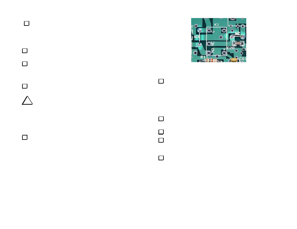
_ Use discarded leads to form jumpers across W2 and W3 near the
outline for K1 as shown in Figure 19. Solder them in place.
Figure 19. Installing W2 and W3 for split path (separate transmit
and receive antenna) operation. Do NOT Install Relay K1
Working around the PCB clockwise from the upper left quadrant,
place the relays at the following locations. They can only be installed one
way. Do not solder the relays yet and do not clip or bend the relay
leads.
__K1
__K8 __K9
__K7
__K4
__K5 __K6 __K2
Using a thin, hardcover book to hold the relays in place, flip the
PCB and book over together.
Solder just two diagonally opposite corner pins on each relay.
Turn the book back over and check each relay. If any relay is not flat
against the PCB, reheat its corner pins while pressing it down against the
PCB.
Once all the relays are properly seated, solder the remaining pins.
Take care to locate and solder all five pins on every relay. Do not trim
the relay pins. Trimming the pins can cause mechanical stress which
may reduce the life of the relay.