I/o pin configuration options, Iocr1 – Rainbow Electronics DS26504 User Manual
Page 52

DS26504 T1/E1/J1/64KCC BITS Element
52 of 128
10. I/O PIN CONFIGURATION OPTIONS
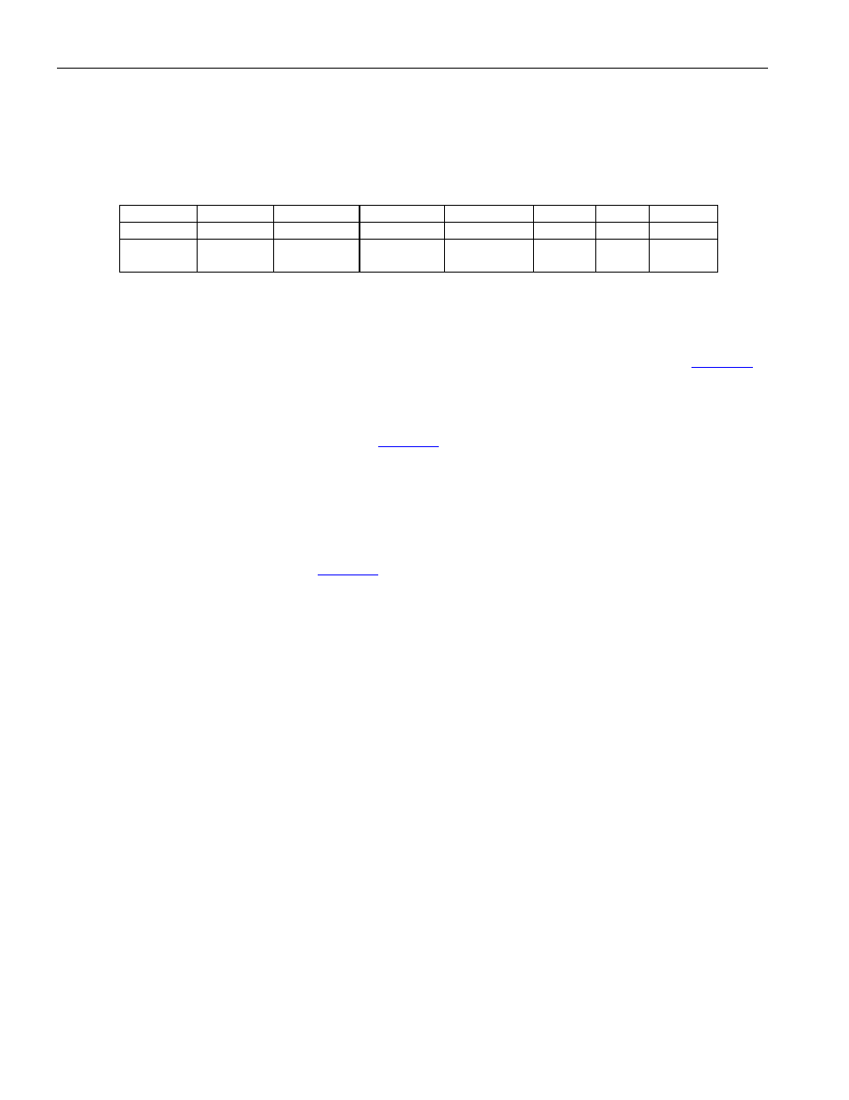
Register Name:
IOCR1
Register Description:
I/O Configuration Register 1
Register Address:
01h
Bit
# 7 6 5 4 3 2
1
0
Name G703TE
RSMS2 RSMS1 RLOFF
CSM_TSDW
TSM TSIO ODF
Default 0
0
0
0
0 0 0 0
HW
Mode
0 0
RSM
PIN 1
0 0
TSM
PIN 2
0 0
Bit 0: Output Data Format (ODF)
0 = bipolar data at TPOS and TNEG
1 = NRZ data at TPOS; TNEG = 0
Bit 1: TS_8K_4 I/O Select (TSIO). This bit determines whether the TS_8K_4 pin is an input or and output. See
0 = TS_8K_4 is an input
1 = TS_8K_4 is an output
Bit 2: TS_8K_4 Mode Select (TSM). In T1 or E1 operation, selects frame or multiframe mode for the TS_8K_4 pin. In
6312kHz or 64KCC mode, this bit should be set = 0. See
0 = frame mode
1 = multiframe mode
Bit 3: Composite Clock Sync Mode_Transmit Signaling Double-Wide Sync (CSM_TSDW). In 64kHz Composite Clock
mode, this bit determines whether the TS_8K_4 pin is an 8kHz or a 400Hz reference input (TS_8K_4 pin in input mode,
IOCR1 = 0), or an 8kHz or 400Hz reference output (TS_8K_4 pin in output mode, IOCR1 = 1). In T1 mode, setting this bit =
1 and setting TSIO = 1 will cause the sync pulse output on TS_8K_4 to be two clocks wide during signaling frames. In E1 or
6312kHz mode, this bit should be set = 0. See
0 = (CC64K) 8kHz reference, (T1) normal sync pulses
1 = (CC64K) 400Hz reference, (T1) double-wide sync pulses during signaling frames
Bit 4: RLOF_CCE Output Function (RLOFF). In T1 or E1 receive mode, this bit determines the function of the
RLOF_CCE pin. In 64KCC or 6312kHz receive mode, this bit should be set = 0.
0 = receive loss of frame (RLOF)
1 = loss-of-transmit clock (LOTC)
Bit 5: RS_8K Mode Select 1(RSMS1). In T1 or E1 receive mode, this bit selects a frame or multiframe output pulse at
RS_8K pin. IOCR.6 may be used to select other functions for the RS_8K pin.
0 = frame mode
1 = multiframe mode
Bit 6: RS_8K Mode Select 2 (RSMS2). In T1 and E1 receive mode, this bit along with IOCR.5 selects the function of the
RS_8K pin.
T1 Mode: (when IOCR.5 set = 0)
0 = do not pulse double-wide in signaling frames
1 = do pulse double-wide in signaling frames
E1 Mode: (when IOCR.5 set = 1)
0 = RS_8K outputs CAS multiframe boundaries
1 = RS_8K outputs CRC4 multiframe boundaries
Bit 7: G.703 Timing Enable (G703TE). Setting this bit causes the 8kHz and 400Hz outputs to have timing relationships to
the 64kHz composite clock signal as specified in G.703. This bit allows backward compatibility with earlier devices in the
DS2650x family. Note: This applies to 64KCC modes only.
0 = legacy timing mode
1 = G.703 timing mode
