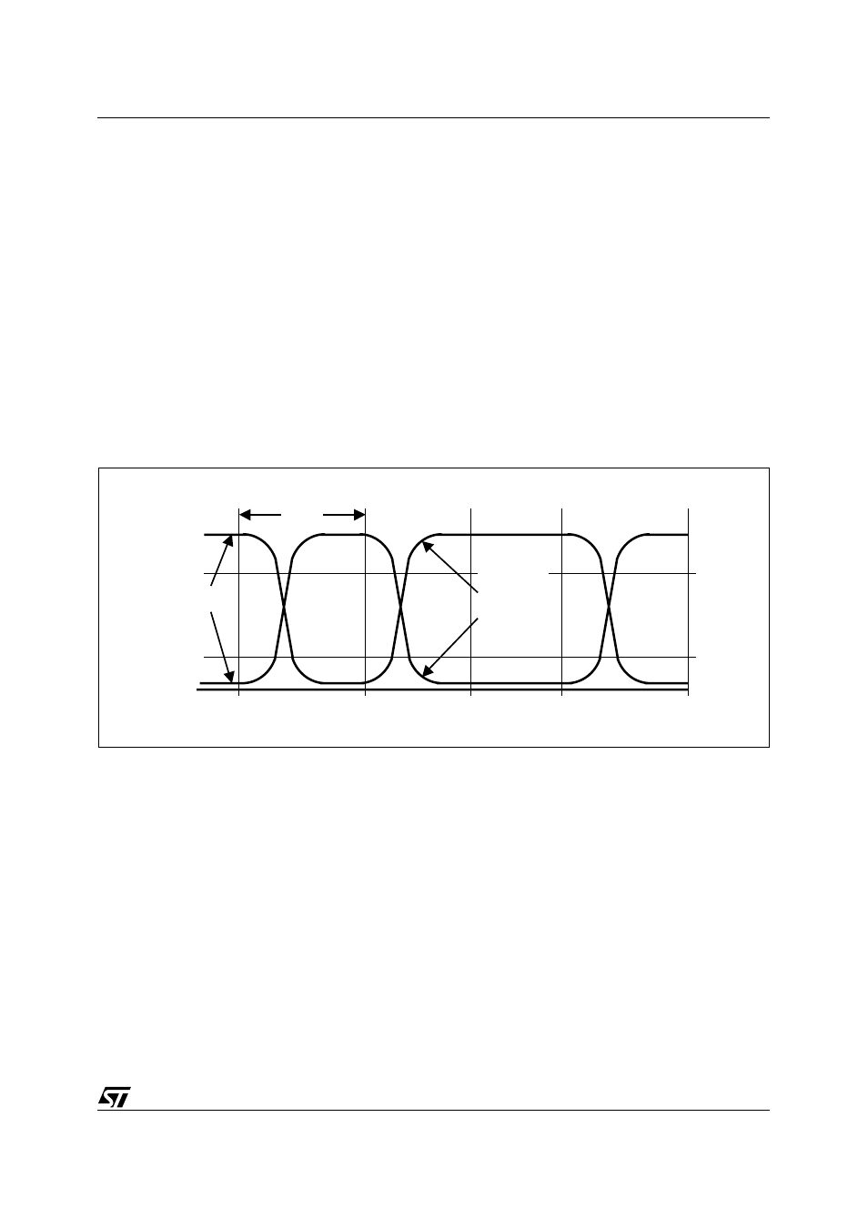
Transceiver, Figure 40. low speed driver signal waveforms – ST & T UPSD3212C User Manual
Page 83

83/163
uPSD3212A, uPSD3212C, uPSD3212CV
Transceiver
USB Physical Layer Characteristics. The fol-
lowing section describes the uPSD321x Devices
compliance to the Chapter 7 Electrical section of
the USB Specification, Revision 1.1. The section
contains all signaling, and physical layer specifica-
tions necessary to describe a low speed USB
function.
Low Speed Driver Characteristics. The
uPSD321x Devices use a differential output driver
to drive the Low Speed USB data signal onto the
USB cable. The output swings between the differ-
ential high and low state are well balanced to min-
imize signal skew. The slew rate control on the
driver minimizes the radiated noise and cross talk
on the USB cable. The driver’s outputs support
three-state operation to achieve bi-directional half
duplex operation. The uPSD321x Devices driver
tolerates a voltage on the signal pins of -0.5V to
3.6V with respect to local ground reference without
damage. The driver tolerates this voltage for
10.0µs while the driver is active and driving, and
tolerates this condition indefinitely when the driver
is in its high impedance state.
A low speed USB connection is made through an
unshielded, untwisted wire cable a maximum of 3
meters in length. The rise and fall time of the sig-
nals on this cable are well controlled to reduce RFI
emissions while limiting delays, signaling skews
and distortions. The uPSD321x Devices driver
reaches the specified static signal levels with
smooth rise and fall times, resulting in segments
between low speed devices and the ports to which
they are connected.
Figure 40. Low Speed Driver Signal Waveforms
AI06629
Signal pins
pass output
spec levels
with minimal
reflections and
ringing
One Bit
Time
1.5 Mb/s
V
SS
Driver
Signal Pins
V
SE
(min)
V
SE
(max)
