Registers, Figure 6. 8032 mcu registers, Figure 7. configuration of ba 16-bit registers – ST & T UPSD3212C User Manual
Page 14: Figure 8. stack pointer

uPSD3212A, uPSD3212C, uPSD3212CV
14/163
Registers
The 8032 has several registers; these are the Pro-
gram Counter (PC), Accumulator (A), B Register
(B), the Stack Pointer (SP), the Program Status
Word (PSW), General purpose registers (R0 to
R7), and DPTR (Data Pointer register).
Accumulator. The Accumulator is the 8-bit gen-
eral purpose register, used for data operation such
as transfer, temporary saving, and conditional
tests. The Accumulator can be used as a 16-bit
register with B Register as shown in Figure
.
B Register. The B Register is the 8-bit general
purpose register, used for an arithmetic operation
such as multiply, division with the Accumulator
(see Figure
Stack Pointer. The Stack Pointer Register is 8
bits wide. It is incremented before data is stored
during PUSH and CALL executions. While the
stack may reside anywhere in on-chip RAM, the
Stack Pointer is initialized to 07h after reset. This
causes the stack to begin at location 08h (see Fig-
ure
).
Program Counter. The Program Counter is a 16-
bit wide which consists of two 8-bit registers, PCH
and PCL. This counter indicates the address of the
next instruction to be executed. In RESET state,
the program counter has reset routine address
(PCH:00h, PCL:00h).
Program Status Word. The Program Status
Word (PSW) contains several bits that reflect the
current state of the CPU and select Internal RAM
(00h to 1Fh: Bank0 to Bank3). The PSW is de-
scribed in
. It contains the Carry
Flag, the Auxiliary Carry Flag, the Half Carry (for
BCD operation), the general purpose flag, the
Register Bank Select Flags, the Overflow Flag,
and Parity Flag.
[Carry Flag, CY]. This flag stores any carry or not
borrow from the ALU of CPU after an arithmetic
operation and is also changed by the Shift Instruc-
tion or Rotate Instruction.
[Auxiliary Carry Flag, AC]. After operation, this is
set when there is a carry from Bit 3 of ALU or there
is no borrow from Bit 4 of ALU.
[Register Bank Select Flags, RS0, RS1]. This flags
select one of four bank(00~07H:bank0,
08~0Fh:bank1, 10~17h:bank2, 17~1Fh:bank3) in
Internal RAM.
[Overflow Flag, OV]. This flag is set to '1' when an
overflow occurs as the result of an arithmetic oper-
ation involving signs. An overflow occurs when the
result of an addition or subtraction exceeds +127
(7Fh) or -128 (80h). The CLRV instruction clears
the overflow flag. There is no set instruction. When
the BIT instruction is executed, Bit 6 of memory is
copied to this flag.
[Parity Flag, P]. This flag reflects on number of Ac-
cumulator’s “1.” If the number of Accumulator’s 1
is odd, P=0. otherwise, P=1. The sum of adding
Accumulator’s 1 to P is always even.
R0~R7. General purpose 8-bit registers that are
locked in the lower portion of internal data area.
Data Pointer Register. Data Pointer Register is
16-bit wide which consists of two-8bit registers,
DPH and DPL. This register is used as a data
pointer for the data transmission with external data
memory in the PSD Module.
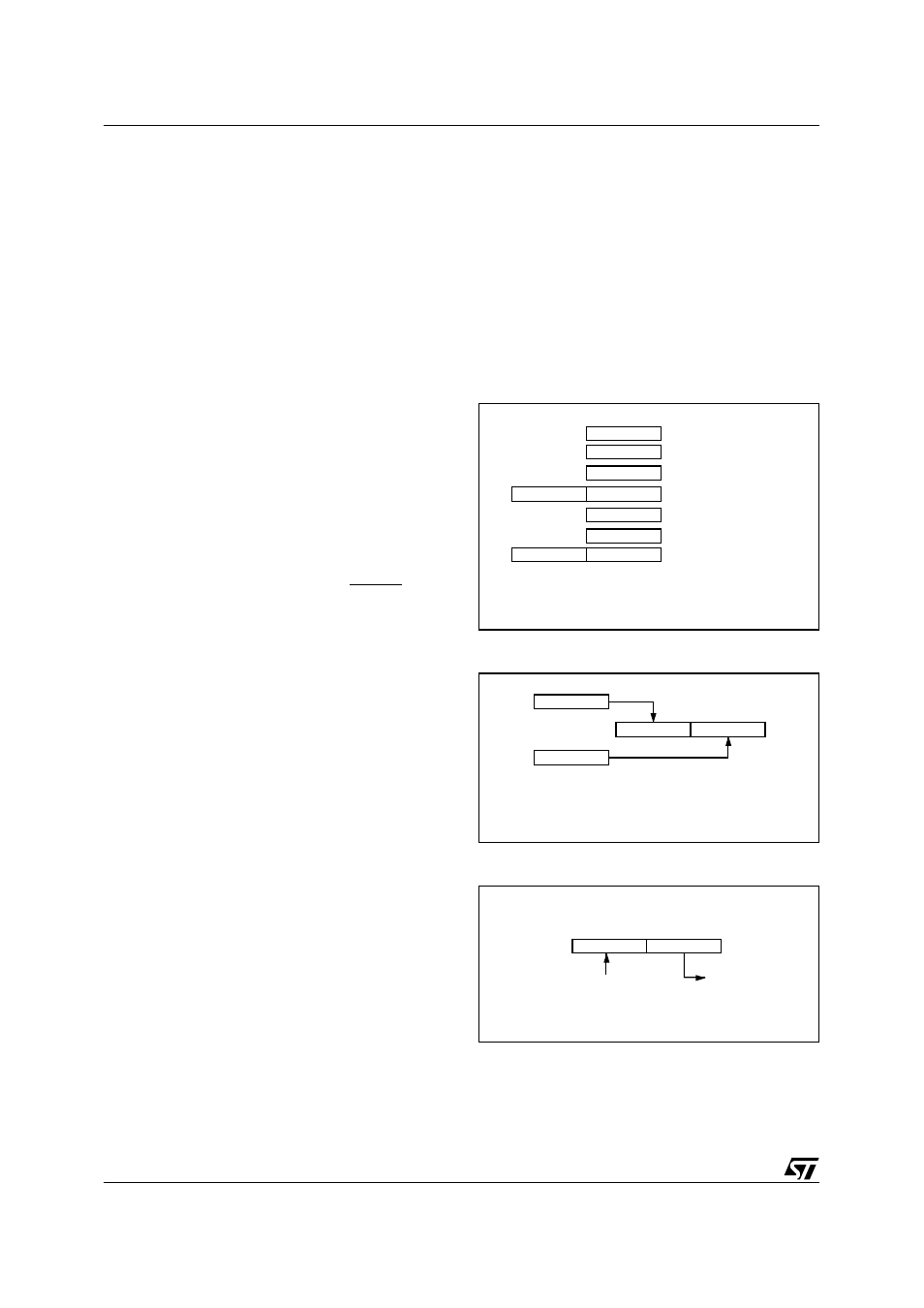
Figure 6. 8032 MCU Registers
Figure 7. Configuration of BA 16-bit Registers
Figure 8. Stack Pointer
AI06636
Accumulator
B Register
Stack Pointer
Program Counter
Program Status Word
General Purpose
Register (Bank0-3)
Data Pointer Register
PCH
DPTR(DPH)
A
B
SP
PCL
PSW
R0-R7
DPTR(DPL)
AI06637
Two 8-bit Registers can be used as a "BA" 16-bit Registers
A
B
A
B
AI06638
SP (Stack Pointer) could be in 00h-FFh
SP
00h
Stack Area (30h-FFh)
00h-FFh
Hardware Fixed
Bit 15
Bit 0
Bit 8 Bit 7
