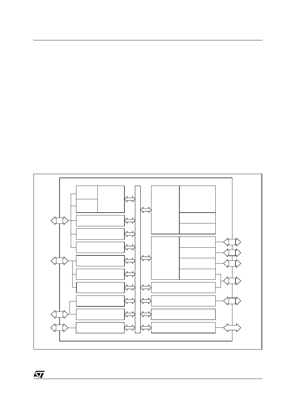
Summary description, Figure 2. block diagram – ST & T UPSD3212C User Manual
Page 7

7/163
uPSD3212A, uPSD3212C, uPSD3212CV
SUMMARY DESCRIPTION
The uPSD321x Series combines a fast 8051-
based microcontroller with a flexible memory
structure, programmable logic, and a rich periph-
eral mix including USB, to form an ideal embedded
controller. At its core is an industry-standard 8032
MCU operating up to 40MHz.
A JTAG serial interface is used for In-System Pro-
gramming (ISP) in as little as 10 seconds, perfect
for manufacturing and lab development.
The USB 1.1 low-speed interface has one Control
Endpoint and two Interrupt endpoints suitable for
HID class drivers.
The 8032 core is coupled to Programmable Sys-
tem Device (PSD) architecture to optimize the
8032 memory structure, offering two independent
banks of Flash memory that can be placed at vir-
tually any address within 8032 program or data ad-
dress space, and easily paged beyond 64K bytes
using on-chip programmable decode logic.
Dual Flash memory banks provide a robust solu-
tion for remote product updates in the field through
In-Application Programming (IAP). Dual Flash
banks also support EEPROM emulation, eliminat-
ing the need for external EEPROM chips.
General purpose programmable logic (PLD) is in-
cluded to build an endless variety of glue-logic,
saving external logic devices. The PLD is config-
ured using the software development tool, PSD-
soft Express, available from the web at
www.st.com/psm, at no charge.
The uPSD321x also includes supervisor functions
such as a programmable watchdog timer and low-
voltage reset.
Figure 2. Block Diagram
PA0:7
PB0:7
PD1:2
PC0:7
MCU
Bus
P4.0:7
P1.0:7
P3.0:7
uPSD321x
SYSTEM B
US
Dedicated
Pins
Supervisor:
Watchdog and Low-Voltage Reset
1st Flash Memory:
64K Bytes
2nd Flash Memory:
16K Bytes
SRAM:
2K Bytes
Programmable
Decode and
Page Logic
General
Purpose
Programmable
Logic,
16 Macrocells
(8) GPIO, Port A
(80-pin only)
(8) GPIO, Port B
(4) GPIO, Port C
(2) GPIO, Port D
JTAG ISP
8032 Address/Data/Control Bus
(80-pin device only)
V
CC
, V
DD
, GND, Reset, Crystal In
8032
MCU
Core
(3) 16-bit
Timer/
Counters
(2)
External
Interrupts
I
2
C
(4) 8-bit ADC
UART0
(8) GPIO, Port 1
(8) GPIO, Port 3
(8) GPIO, Port 4
UART1
(5) 8-bit PWM
AI10428b
USB+,
USB–
USB v1.1
