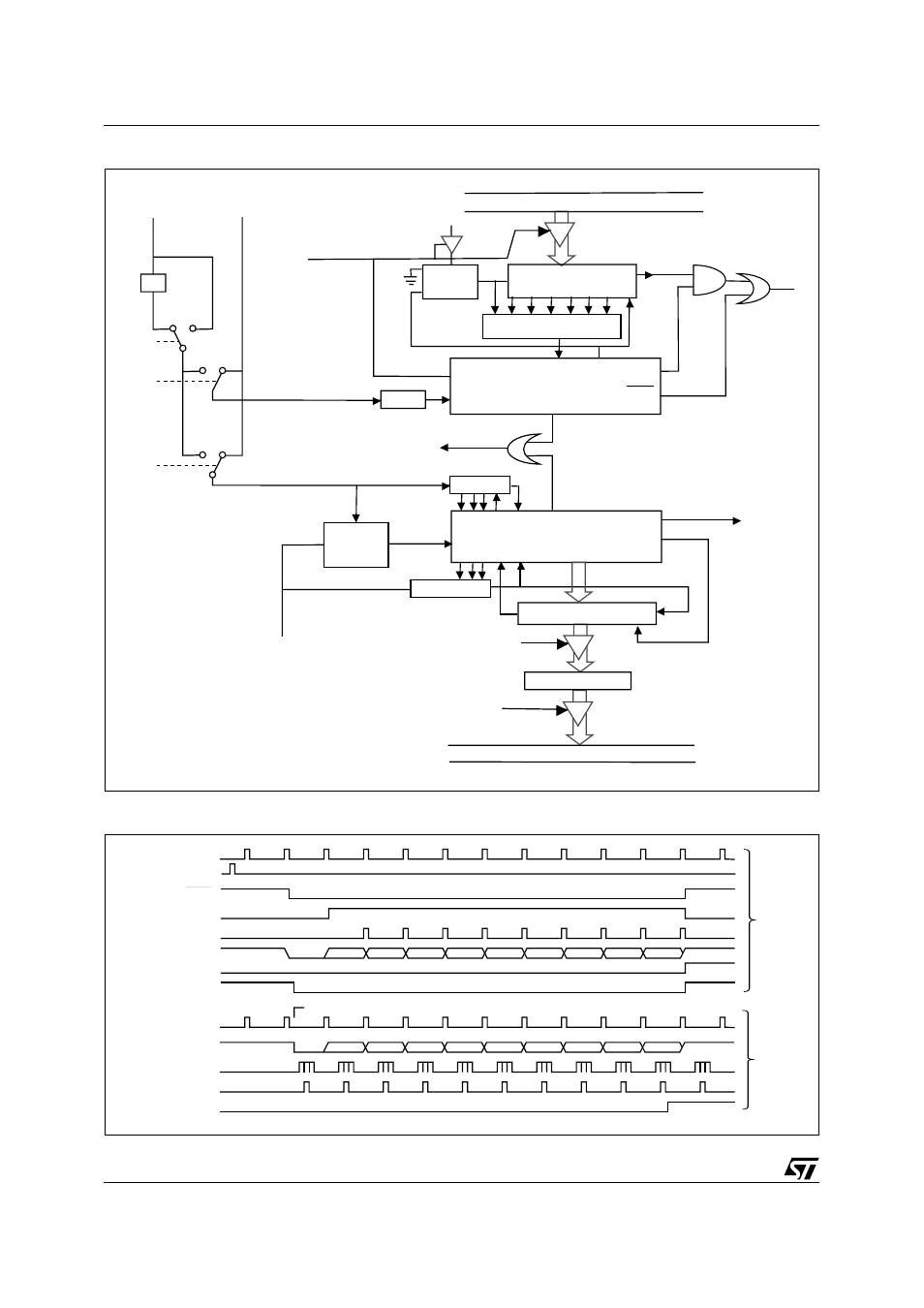
Figure 33. serial port mode 3, block diagram, Figure 34. serial port mode 3, waveforms – ST & T UPSD3212C User Manual
Page 64

uPSD3212A, uPSD3212C, uPSD3212CV
64/163
Figure 33. Serial Port Mode 3, Block Diagram
Figure 34. Serial Port Mode 3, Waveforms
AI06846
Zero Detector
Internal Bus
Tx Control
Rx Control
Internal Bus
SBUF
Write
to
SBUF
Read
SBUF
Load
SBUF
SBUF
Input Shift Register
Shift
Serial
Port
Interrupt
Rx Clock
Start
Tx Clock
Start
Shift
Shift
Send
Load SBUF
TI
RI
CL
D
S
Q
1FFh
TxD
Data
Rx Detector
RxD
1-to-0
Transition
Detector
÷16
Sample
ч16
ч2
TB8
Timer1
Overflow
Timer2
Overflow
0
0
1
1
0
1
TCLK
RCLK
SMOD
AI06847
Write to SBUF
Data
Shift
TxD
TI
Rx Clock
RxD
Bit Detector
Sample Times
Shift
RI
S1P1
÷16 Reset
Receive
Transmit
D0
D1
D2
D3
D4
D5
D6
D7
Send
Tx Clock
Start Bit
Stop Bit
TB8
D0
D1
D2
D3
D4
D5
D6
D7
Start Bit
Stop Bit
RB8
Stop Bit
Generator
This manual is related to the following products:
