7 optical module and i2c ac timing specification, 1 i2c interface timing, Figure 45. bus timing diagram – Intel IXF1104 User Manual
Page 147: Figure 46. write cycle diagram, Optical module and i, Bus timing diagram, Write cycle diagram, 7 optical module and i, C ac timing specification, C interface timing
Intel
®
IXF1104 4-Port Gigabit Ethernet Media Access Controller
147
Datasheet
Document Number: 278757
Revision Number: 009
Revision Date: 27-Oct-2005
7.7
Optical Module and I
2
C AC Timing Specification
7.7.1
I
2
C Interface Timing
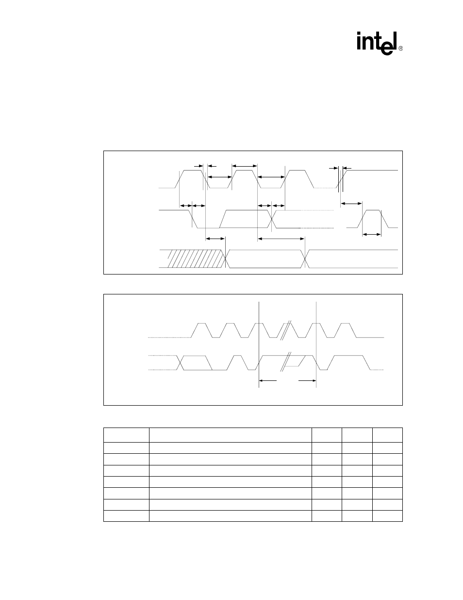
and
illustrate bus timing and write cycle, and
shows the I
2
C Interface
AC timing characteristics.
Figure 45. Bus Timing Diagram
Figure 46. Write Cycle Diagram
Table 53. I
2
C AC Timing Characteristics (Sheet 1 of 2)
Symbol
Parameter
Min
Max
Units
f
SCL
Clock frequency, SCL
-
100
kHz
t
LOW
Clock pulse width low
4.7
µs
t
HIGH
Clock pulse width High
4.0
µs
t
I
Noise suppression
100
µs
t
AA
Clock low to data valid out
0.1
4.5
µs
t
BUF
Time the bus must be free before a new transmission starts
4.7
-
µs
t
HD.STA
Start hold time
4.0
-
µs
I
2
C_Clk
I
2
C_Data Out
t
DH
t
SV.SAT
t
AA
t
BUF
t
HD.STA
t
HIGH
t
R
t
SU.STO
t
SU.DAT
t
HD.DAT
t
LOW
t
F
I
2
C_Data In
t
LOW
ACK
8th
BIT
WORD n
I
2
C_Clk
I
2
C_Data
STOP
CONDITION
START
CONDITION
t WR(1)