2 led interface signal description, Table 31. led interface signal descriptions, 3 mode 0: detailed operation – Intel IXF1104 User Manual
Page 116: Figure 29. mode 0 timing, Led interface signal description, Mode 0: detailed operation, Mode 0 timing, Led interface signal descriptions
Intel
®
IXF1104 4-Port Gigabit Ethernet Media Access Controller
Datasheet
116
Document Number: 278757
Revision Number: 009
Revision Date: 27-Oct-2005
5.8.2
LED Interface Signal Description
The IXF1104 MAC LED interface consists of three output signal signals that are 2.5 V CMOS
level pads.
provides LED signal names, pin numbers, and descriptions.
5.8.3
Mode 0: Detailed Operation
Note:
Please refer to the SGS Thompson* M5450 datasheet for device-operation information.
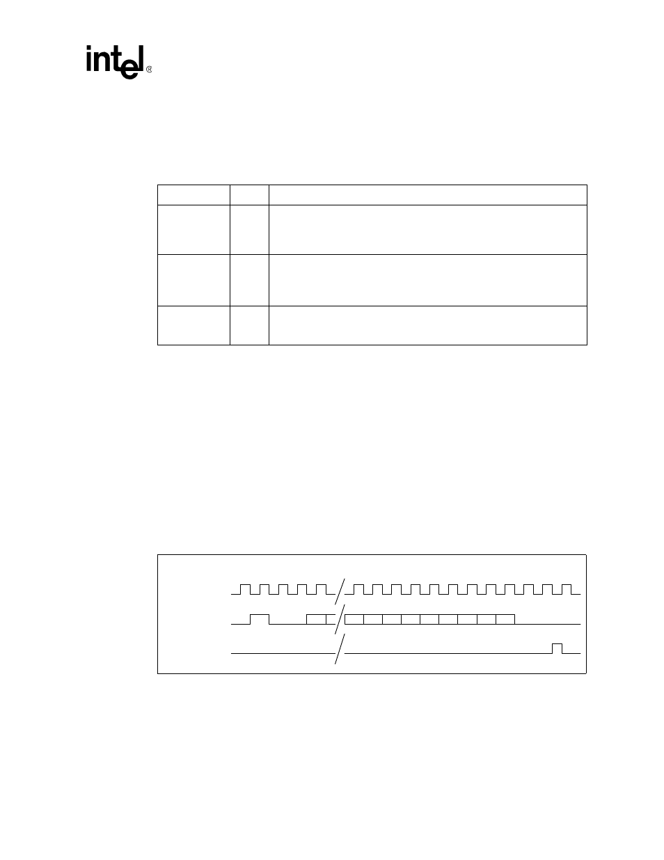
The operation of the LED Interface in Mode 0 is based on a 36-bit counter loop. The data for each
LED is placed in turn on the serial data line and clocked out by the LED_CLK.
shows the
basic timing relationship and relative positioning in the data stream of each bit.
shows the 36 clocks that are output on the LED_CLK pin. The data is changed on the
falling edge of the clock and is valid for almost the entire clock cycle. This ensures that the data is
valid during the rising edge of the LED_CLK, which clocks the data into the M5450 device.
The actual data shown in
consists of a chain of 36 bits, 12 of which are valid LED
DATA. The 36-bit data chain is built up as follows:
Table 31. LED Interface Signal Descriptions
Pin Name
Pin #
Pin Description
LED_CLK
K24
This signal is an output that provides a continuous clock synchronous to the
serial data stream output on the LED_DATA pin. This clock has a maximum
speed of 720 Hz.
The behavior of this signal remains constant in all modes of operation.
LED_DATA
M22
This signal provides the data, in various formats, as a serial bit stream. The data
must be valid on the rising edge of the LED_CLK signal.
In Mode 0, the data presented on this pin is TRUE (Logic 1 = High).
In Mode 1, the data presented on this pin is INVERTED (Logic 1 = Low).
LED_LATCH
L22
This is an output pin, and the signal is used only in Mode 1 as the Latch enable
for the shift register chain.
This signal is not used in Mode 0, and should be left unconnected.
Figure 29. Mode 0 Timing
1
22 23 24 25 26 27 28 29 30
1
35
34
33
32
31
30
29
28
27
26
25
2
3
4
LED_CLK
LED_DATA
LED_LATCH