3 word alignment, Word alignment, Data restrictions on word alignment – FUJITSU FR family 32-bit microcontroller instruction manuel CM71-00101-5E User Manual
Page 35

11
CHAPTER 2 MEMORY ARCHITECTURE
2.3
Word Alignment
In the FR family, the type of data length used determines restrictions on the
designation of memory addresses (word alignment).
■
Program Restrictions on Word Alignment
When using half-word instruction length, memory addresses must be accessed in multiples of two. With
branching instructions and other instructions that may result in attempting to store odd numbered values to
the "PC", the lowest value in the "PC" will be read as "0". Thus an even numbered address will always be
generated by fetching a branching instruction.
■
Data Restrictions on Word Alignment
●
Word data
Data must be assigned to addresses that are multiples of 4. Even if the operand value is not a multiple of 4,
the lower two bits of the memory address will explicitly be read as "0".
●
Half-word data
Data must be assigned to addresses that are multiples of 2. Even if the operand value is not a multiple of 2,
the lowest bit of the memory address will explicitly be read as "0".
●
Byte data
There are no restrictions on addresses.
The forced setting of some bits to "0" during memory access for word data and half-word data is applied
after the computation of the execution address, not at the source of the address information.
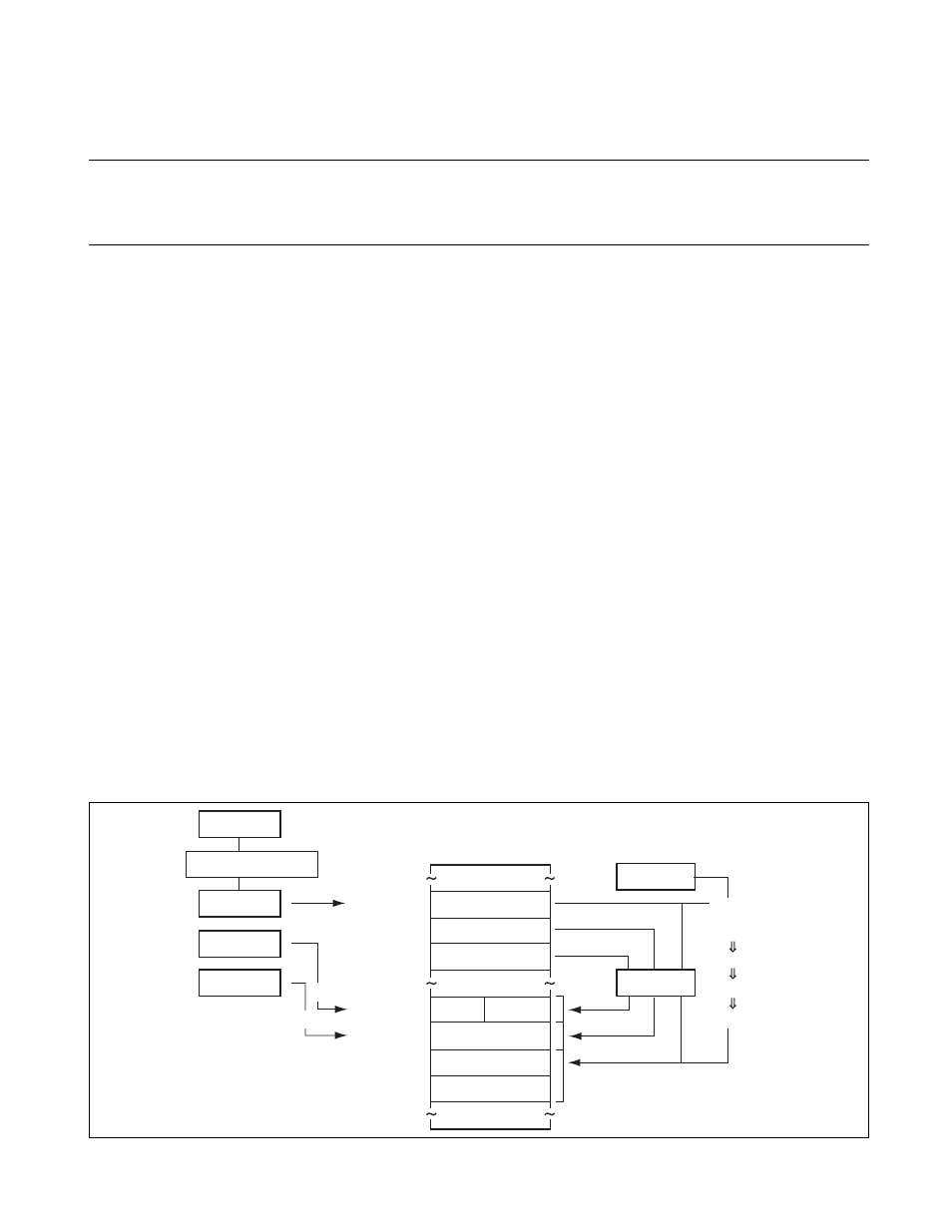
Figure 2.3-1 shows an example of the program-word boundary and data-word boundary.
Figure 2.3-1 Example of Program-word Boundary and Data-word Boundary
CDEF
H
8
9AB
H
CDEF
H
S
T R1
3
,@(R14,4)
S
TH R1
3
,@R2
S
TB R1
3
,@R1
EF
H
0000 0000
H
12
3
4 567
8
H
12
3
4567
8
H
12
3
4 567A
H
4
3
215679
H
12
3
4 567C
H
4
3
21 567A
H
4
3
21 567C
H
4
3
21 567E
H
4
3
21 567
8
H
4
3
21567B
H
FFFF FFFF
H
R10
12
3
45679
H
JMP @R10 : Bit 0 = 0
as
it i
s
Bit 0 = 0
PC
R1
R2
4
3
21567B
H
8
9ABCDEF
H
R14
R1
3
4
3
21567B
H
00000004
H
4
3
21567F
H
4
3
21567C
H
Bit
s
1, 0 = 0
+
Memory
s
p
a
ce
