7 internal block diagram, The m5 drive internal block diagram is shown below, Fig 13.59 internal block diagram – Yaskawa Varispeed 626M5 User Manual
Page 301
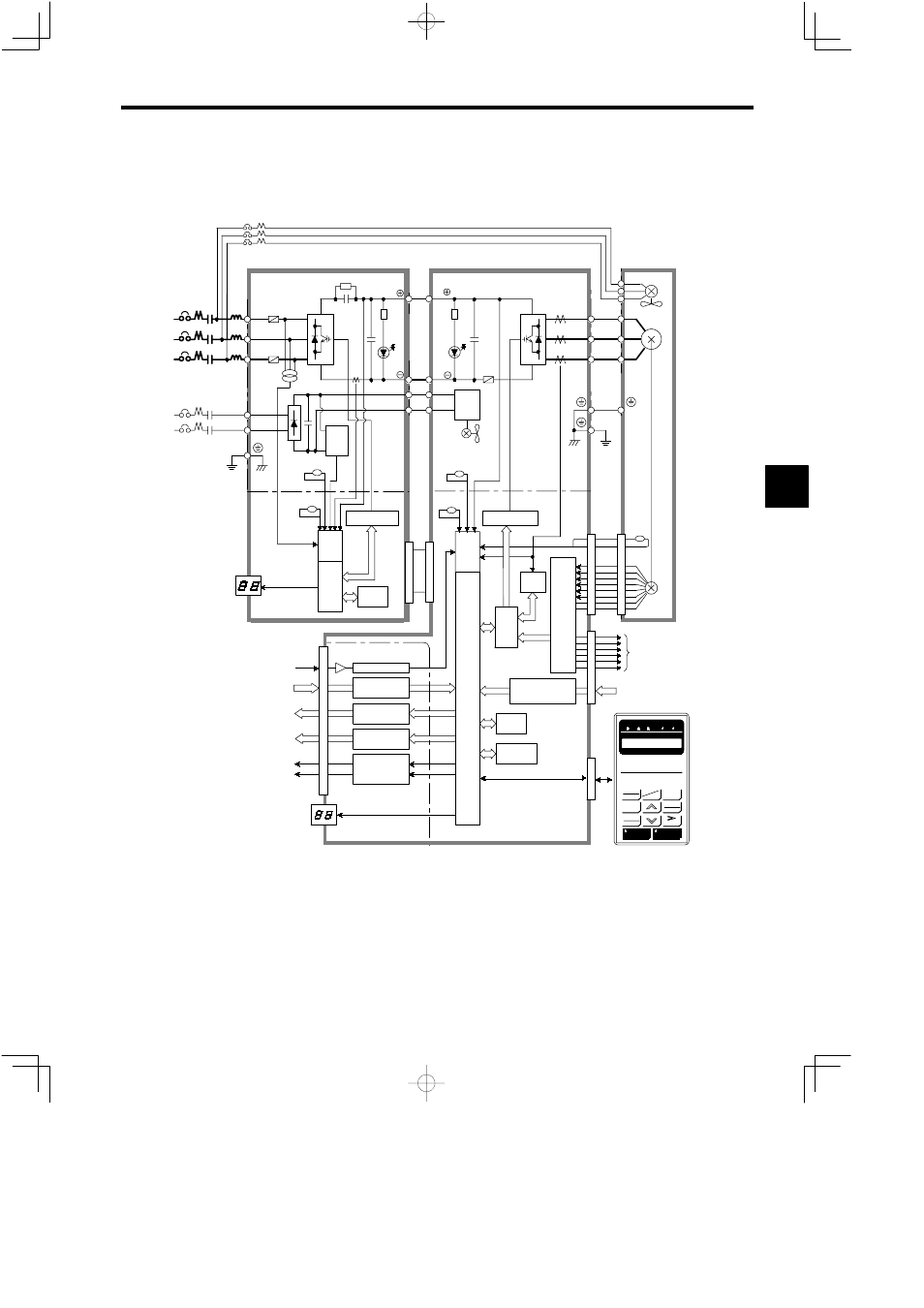
15.7 Internal Block Diagram
15 -29
15.7 Internal Block Diagram
The M5 Drive internal block diagram is shown below.
A2/t
Speed reference (AD)
Sequence outputs
(DO)
Error codes
(DO)
Speedometer signals
Load meter signals
(AO)
P1
Control
power
supply
(RCC)
N1
Gate driver
Detector
(AD)
CPU
TS
TS
P−ROM
5CN
P1
Power
supply
(RCC)
N1
51CN
P/
N/
Internal cooling
fan
Gate driver
TS
TS
Detector
(AD)
DSP
Detector
(AD)
Analog speed reference (±10 V)
Sequence inputs (14 points)
Sequence outputs (10 points)
EEPROM
(Constants)
Motor encoder
signal outputs
Speedometer output (10 V)
Load meter output (10 V)
PG
pulse
proces-
sor
(DIO)
12-bit digital references
(12 points)
1CN
2CN
TS
3CN
Error codes (4 points)
I/O Card (See note.)
6CN
U
V
W
U/T1
V/T2
W/T3
N/
P/
R/L1
S/L2
T/L3
A1/r
VS-656MR5 Converter
VS-626M5 Inverter
+
+
Cooling fan
Motor
12-bit digital refer-
ences (DI)
Digital Operator
PG
+
PROM
Z1
Z2
Z3
R
S
T
1MCCB 1MC
L
3MCCB
2MCCB 2MC
r
t
Sequence inputs
(DI)
CPU
DRIVEFWDREVREMOTE
REF
SEQ
DIGITAL OPERATOR
JVOP−132
REMOTE
LOCAL
PRGM
DRIVE
DSPL
RESET
JOG
ENTER
DATA
RUN
STOP
REMOTE
LOCAL
* An I/O Card is mounted when using an M5A Independent Drive
Fig 13.59
Internal Block Diagram
15