Measurement Computing Data Acquisition Systems rev.10.4 User Manual
Page 203
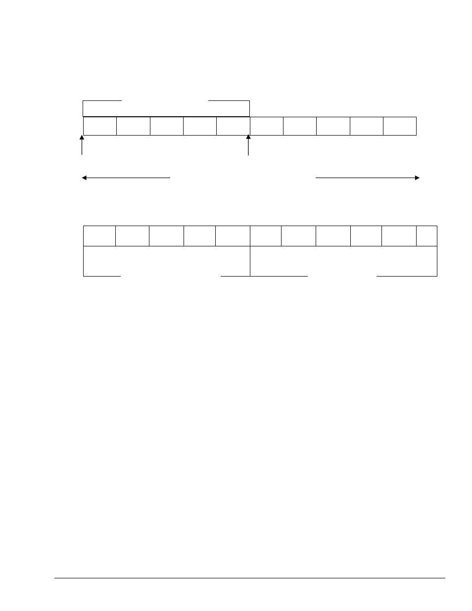
The transfer output buffer is organized into update data blocks. When the output update clock fires, the next
available update data block is loaded from the internal waveform/pattern output FIFO on the device to the port,
which then presents the values to either the DAC or digital port for output.
DAC0 DAC1 DAC2 DAC3 P3D0 DAC0 DAC1 DAC2 DAC3 P3D0
Data Presented to Outputs
Update clock
Update clock
Likewise, the buffer is organized in a similar manner.
DAC0 DAC1 DAC2 DAC3 P3D0 DAC0 DAC1 DAC2 DAC3 P3D0 …
Update Data Block 0
Update Data Block 1
Processing Output FIFO
As the output FIFO empties, the driver will automatically transfer data from the output transfer buffer to the
output FIFO on the device. This transfer process will continue until either the waveform/pattern output
transfer is stopped via the daqDacTransferStop function, the waveform/pattern output is halted with the
daqDacWaveDisarm
function or the waveform/pattern output is normally terminated as defined by the
daqDacWaveSetMode
function.
Buffer Output Channel Data Format
The format for each update sample in the buffer is a 16-bit integer. This parameter is an integer value ranging
from 0 to 65,535. This is a 16-bit value and the 16-bit value spans the range over which the output can vary,
depending upon the specified range of the port for the device.
Some DAC channels use 16-bit D/A converters--in these converters, each bit in the 16-bit integer corresponds
to one bit programmed to the D/A converter. However, some DAC channels have 12-bit D/A converters. In
this case, the low order nibble (4-bits) of the 16-bit sample will be ignored.
The specifications section of the device user’s manual provides the ranges and the associated resolution values
for the device.
Programmer’s Manual
908494
Daq API Command Reference 4.4-21