1 input/output amplifier overview, 2 amplifier control register descriptions, 1 amplifier control register (ampcn, m3[06h]) – Maxim Integrated MAXQ Family Users Guide: MAXQ8913 Supplement User Manual
Page 98: 1 amplifier control register (ampcn, m3[06h]) -1, Maxq family user’s guide: maxq8913 supplement, Table 24-1. amplifier control registers
MAXQ Family User’s Guide:
MAXQ8913 Supplement
24-1
SECTION 24: INPUT/OUTPUT AMPLIFIERS (SPECIFIC TO
MAXQ8913)
24.1 Input/Output Amplifier Overview
The MAXQ8913 controls two amplifier stages as described in this section. The input amplifier stage consists of four
internal, uncommitted op amps that can be used to amplify and/or filter the inputs to the ADC. The output stage con-
sists of an external Class D amplifier that can be used to postprocess the outputs from DAC1 and DAC2.
24.2 Amplifier Control Register Descriptions
Addresses of registers are given as “Mx[yy],” where x is the module number (from 0 to 15 decimal) and yy is the reg-
ister index (from 00h to 1Fh hexadecimal). Fields in the bit definition tables are defined as follows:
• Name: Symbolic names of bits or bit fields in this register.
• Reset: The value of each bit in this register following a standard reset. If this field reads “unchanged,” the given bit
is unaffected by standard reset. If this field reads “s,” the given bit does not have a fixed 0 or 1 reset value because
its value is determined by another internal state or external condition.
• POR: If present this field defines the value of each bit in this register following a power-on reset (as opposed to a
standard reset). Some bits are unaffected by standard resets and are set/cleared by POR only.
• Access: Bits can be read-only (r) or read/write (rw). Any special restrictions or conditions that could apply when
reading or writing this bit are detailed in the bit description.
24.2.1 Amplifier Control Register (AMPCN, M3[06h])
Bit 7: Reserved. All reads return 0.
Bit 6: Amplifier Fault Flag (AMPFLT). This bit is set to 0 by hardware when the FAULT input from the external
D-amplifier goes low. It is set to 1 by hardware whenever FAULT is high, or when both amplifiers are disabled (AMPEN0
= 0 and AMPEN1 = 0), or when the amplifier clock is disabled (AMPCK[1:0] == 00b).
Bit 5: Amplifier Interrupt Flag (AMPIF). If this bit is set to 1, an interrupt is generated if AMPIE = 1. This bit is set to 1
by hardware when the AMPFLT flag changes from 1 to 0. This bit must be cleared by software once set.
Bit 4: Amplifier Interrupt Enable (AMPIE). If this bit is set to 1, an interrupt is generated when AMPIF = 1. If this bit
is set to 0, amplifier interrupts are disabled.
Bits 3:2: Amplifier Clock Divide (AMPCK[1:0]). These two bits control the D-amplifier clock output that is generated
on the SYNCIN pin. This clock is generated from a divided-down version of the system clock as follows:
AMPCK1 = 0, AMPCK0 = 0: No output clock (disabled).
AMPCK1 = 0, AMPCK0 = 1: SYNCIN clock = System clock divided by 2.
AMPCK1 = 1, AMPCK0 = 0: SYNCIN clock = System clock divided by 3.
AMPCK1 = 1, AMPCK0 = 0: SYNCIN clock = System clock divided by 4.
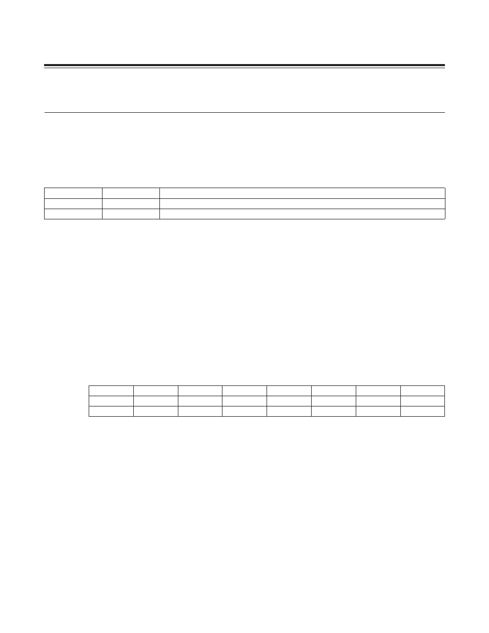
Table 24-1. Amplifier Control Registers
REGISTER
ADDRESS
FUNCTION
AMPCN
M3[06h]
Amplifier Control Register. Controls the external Class-D amplifier.
OPMCN
M3[0Ah]
Op Amp Control Register. Enables/disables the internal uncommitted op amps.
Bit #
7
6
5
4
3
2
1
0
Name
—
AMPFLT
AMPIF
AMPIE
AMPCK1
AMPCK0
AMPEN1
AMPEN0
Reset
0
1
0
0
0
0
0
0
Access
r
r
rw
rw
rw
rw
rw
rw
Maxim Integrated