4 adc data register (addata, m3[09h]), Maxq family user’s guide: maxq8913 supplement – Maxim Integrated MAXQ Family Users Guide: MAXQ8913 Supplement User Manual
Page 69
MAXQ Family User’s Guide:
MAXQ8913 Supplement
19-7
Bits 3:0: ADC Sample Acquisition Time Extend (ADACQ[3:0]). These bits set the extended sample acquisition time
period. For a given conversion, sample acquisition time is extended if the ADACQEN bit is set in the conversion con-
figuration (ADCFG) register. If this bit is set, the acquisition time is extended by:
16 x (ADACQ[3:0] + 1) x ADC clock period
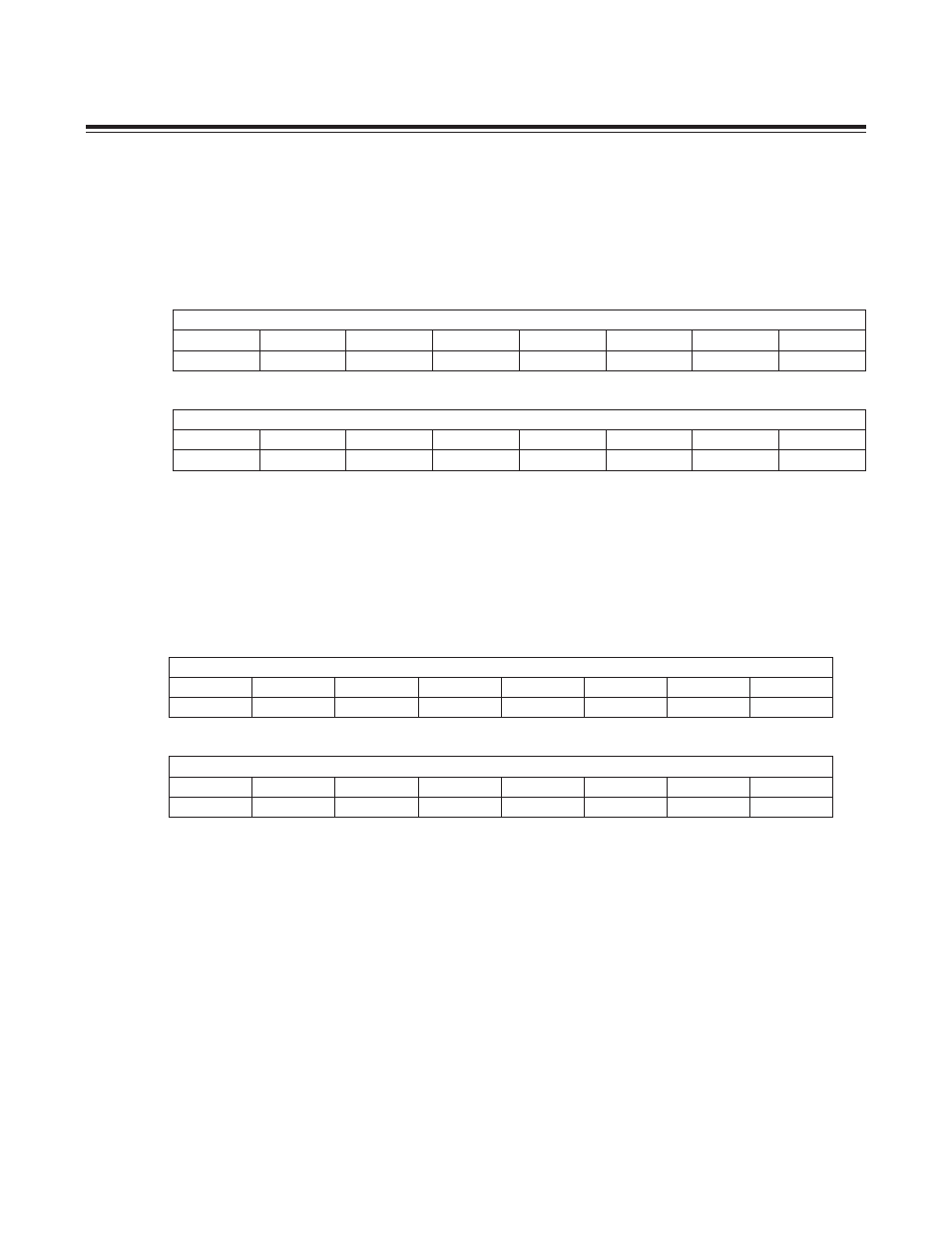
19.2.4 ADC Data Register (ADDATA, M3[09h])
This register is an access point for the eight ADC configuration registers (ADCFG[0] to ADCFG[7]) and 16 ADC data
buffer registers (ADBUF[0] to ADBUF[15]). Reading or writing ADDATA actually reads or writes the selected register,
as determined by ADST[4:0].
19.2.5 ADC Data Buffer Registers (ADBUF[0] to ADBUF[15], ADDATA[00h] to ADDATA[0Fh])
The 16 ADC data buffer registers ADBUF[0] to ADBUF[15] serve as temporary holding storage for ADC conversion
samples until the samples can be read by the processor. They can be read or written at any time, whether or not an
ADC conversion is in progress.
As each ADC conversion completes, the resulting sample is written to one of the ADBUF registers, starting with the
index given by SEQSTORE (ADADDR[11:8]) and incrementing from there with each new sample written. The index of
the most recent ADBUF register written to by the ADC controller is always available in the ADDAT bit field (ADST[11:8]).
The ADC samples are written into the ADBUF registers in either left-aligned or right-aligned format as selected by
the ADALGN bit for that conversion configuration register. Once a sample is written into an ADBUF register, the data
remains there until it is erased by software or until it is overwritten by another ADC sample, 16 conversions later. When
continuous-conversion mode is used, it is the responsibility of the user software to monitor the data available interrupt
and read ADC samples from the ADBUF registers before they are overwritten by subsequent samples.
Note: The effect of read or write operation depends on ADIDX and ADCFG bit settings.
Bit #
15
14
13
12
11
10
9
8
Name
ADDATA
Reset
s
s
s
s
s
s
s
s
Access
rw
rw
rw
rw
rw
rw
rw
rw
Bit #
7
6
5
4
3
2
1
0
Name
ADDATA
Reset
s
s
s
s
s
s
s
s
Access
rw
rw
rw
rw
rw
rw
rw
rw
Bit #
15
14
13
12
11
10
9
8
Name
ADBUF
Reset
0
0
0
0
0
0
0
0
Access
rw
rw
rw
rw
rw
rw
rw
rw
Bit #
7
6
5
4
3
2
1
0
Name
ADBUF
Reset
0
0
0
0
0
0
0
0
Access
rw
rw
rw
rw
rw
rw
rw
rw
Maxim Integrated