Maxq family user’s guide: maxq8913 supplement, Table 4-1. system register map, Table 4-2. system register bit functions – Maxim Integrated MAXQ Family Users Guide: MAXQ8913 Supplement User Manual
Page 23
MAXQ Family User’s Guide:
MAXQ8913 Supplement
4-1
ADDENDUM TO SECTION 4: SYSTEM REGISTER DESCRIPTIONS
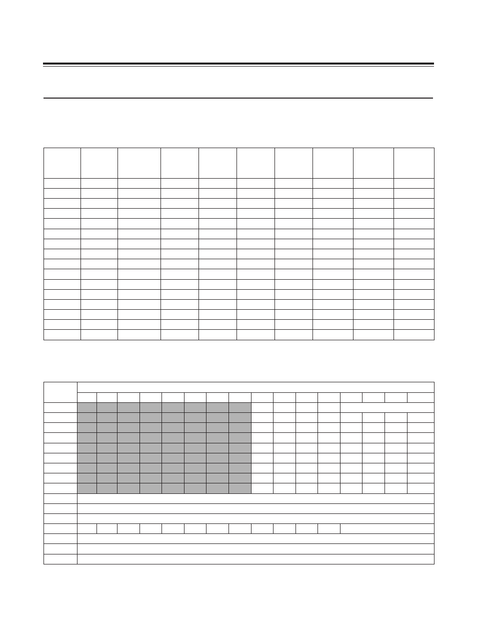
Refer to Section 4: System Register Descriptions of the MAXQ Family User’s Guide for functional descriptions of the
registers and bits in Table 4-1.
Table 4-1. System Register Map
Note: Register names that appear in italics indicate read-only registers. Register names that appear in bold indicate 16-bit regis-
ters. All other registers are 8 bits in width.
Table 4-2. System Register Bit Functions
CYCLES
TO
READ
CYCLES
TO
WRITE
REGISTER
INDEX
AP
(M8)
A
(M9)
PFX
(M11)
IP
(M12)
SP
(M13)
DPC
(M14)
DP
(M15)
1
1
00h
AP
A[0]
PFX[0]
IP
—
—
—
1
1
01h
APC
A[1]
PFX[1]
—
SP
—
—
1
1
02h
—
A[2]
PFX[2]
—
IV
—
—
1
1
03h
—
A[3]
PFX[3]
—
—
OFFS
DP[0]
1
1
04h
PSF
A[4]
PFX[4]
—
—
DPC
—
1
1
05h
IC
A[5]
PFX[5]
—
—
GR
—
1
1
06h
IMR
A[6]
PFX[6]
—
LC[0]
GRL
—
1
1
07h
—
A[7]
PFX[7]
—
LC[1]
BP
DP[1]
1
2
08h
SC
A[8]
—
—
—
GRS
—
1
2
09h
—
A[9]
—
—
—
GRH
—
1
2
0Ah
—
A[10]
—
—
—
GRXL
—
1
2
0Bh
IIR
A[11]
—
—
—
BP[OFFS]
—
1
2
0Ch
—
A[12]
—
—
—
—
—
1
2
0Dh
—
A[13]
—
—
—
—
—
1
2
0Eh
CKCN
A[14]
—
—
—
—
—
1
2
0Fh
WDCN
A[15]
—
—
—
—
—
REG
BIT
15
14
13
12
11
10
9
8
7
6
5
4
3
2
1
0
AP
—
—
—
—
AP (4 bits)
APC
CLR
IDS
—
—
—
MOD2 MOD1 MOD0
PSF
Z
S
—
GPF1 GPF0
OV
C
E
IC
—
—
—
—
—
—
INS
IGE
IMR
IMS
—
—
—
IM3
IM2
IM1
IM0
SC
TAP
—
—
CDA0
—
—
PWL
—
IIR
IIS
—
—
—
II3
II2
II1
II0
CKCN
—
RGSL RGMD STOP SWB PMME CD1
CD0
WDCN
POR EWDI WD1
WD0 WDIF WTRF EWT
RWT
A[0:15]
A[0:15] (16 bits)
PFX
PFX (16 bits)
IP
IP (16 bits)
SP
—
—
—
—
—
—
—
—
—
—
—
—
SP (4 bits)
IV
IV (16 bits)
LC[0]
LC[0] (16 bits)
LC[1]
LC[1] (16 bits)
Maxim Integrated