1 i2c register descriptions, Section 22 : i, C bus interface (specific to maxq8913) – Maxim Integrated MAXQ Family Users Guide: MAXQ8913 Supplement User Manual
Page 87: C register descriptions -1, Maxq family user’s guide: maxq8913 supplement, Register descriptions, Table 22-1. i, C input and output pins table 22-2. i, C interface control registers
MAXQ Family User’s Guide:
MAXQ8913 Supplement
22-1
SECTION 22 : I
2
C BUS INTERFACE (SPECIFIC TO MAXQ8913)
The MAXQ8913 provides an inter-IC (I
2
C) communications module that includes master and slave modes. The associ-
ated pins and registers for this interface are listed in Table 22-1 and Table 22-2.
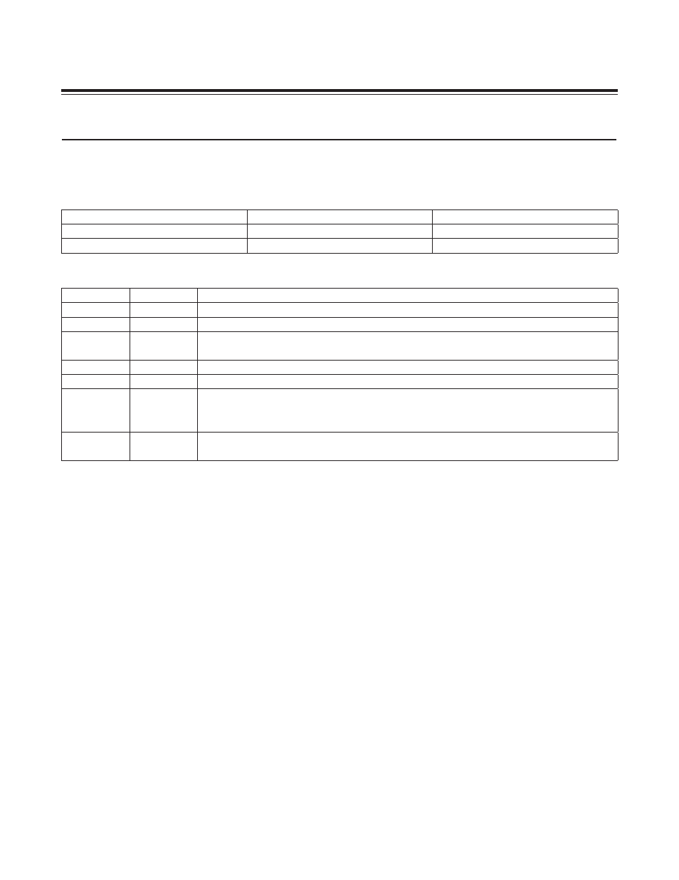
Table 22-1. I
2
C Input and Output Pins
Table 22-2. I
2
C Interface Control Registers
22.1
I
2
C
Register Descriptions
The following peripheral registers are used to control the integrated I
2
C peripheral on the MAXQ8913. Addresses for
all registers are given as “Mx[yy],” where x is the module number (from 0 to 15 decimal) and yy is the register index
(from 00h to 1Fh hexadecimal). Fields in the bit definition tables are defined as follows:
• Name: Symbolic names of bits or bit fields in this register.
• Reset: The value of each bit in this register following a standard reset. If this field reads “unchanged,” the given bit
is unaffected by standard reset. If this field reads “s,” the given bit does not have a fixed 0 or 1 reset value because
its value is determined by another internal state or external condition.
• POR: If present this field defines the value of each bit in this register following a power-on reset (as opposed to a
standard reset). Some bits are unaffected by standard resets and are set/cleared by POR only.
• Access: Bits can be read-only (r) or read/write (rw). Any special restrictions or conditions that could apply when
reading or writing this bit are detailed in the bit description.
I
2
C INTERFACE FUNCTION
PIN
MULTIPLEXED WITH GPIO
SCL: Clock
N4
P1.0
SDA: Data
M3
P1.1
REGISTER
ADDRESS
FUNCTION
I2CBUF
M1[06h]
I
2
C Data Buffer Register. Interface register for the input and output I
2
C buffers.
I2CST
M1[05h]
I
2
C Status Register. Contains the interrupt and status flags for the I
2
C interface.
I2CIE
M1[07h]
I
2
C Interrupt Enable Register. Contains the interrupt-enable bits and control bits for general call
address matching and clock stretching.
I2CCN
M1[04h]
I
2
C Control Register. Contains the control and configuration bits for the I
2
C interface.
I2CCK
M1[0Ch]
I
2
C Clock Control Register. Defines the SCL high and low clock periods for I
2
C master mode.
I2CTO
M1[0Dh]
I
2
C Timeout Register. Enables/disables the master mode timeout when the bus is busy or SCL
is held low by another device longer than the maximum allowed time, and defines the timeout
period.
I2CSLA
M1[0Eh]
I
2
C Slave Address Register. Defines the 7-bit/10-bit address that is recognized by the slave
portion of the I
2
C interface.
Maxim Integrated