1 analog-to-digital converter features, 1 analog-to-digital converter features -1, Maxq family user’s guide: maxq8913 supplement – Maxim Integrated MAXQ Family Users Guide: MAXQ8913 Supplement User Manual
Page 63
MAXQ Family User’s Guide:
MAXQ8913 Supplement
19-1
SECTION 19: ANALOG-TO-DIGITAL CONVERTER (SPECIFIC TO
MAXQ8913)
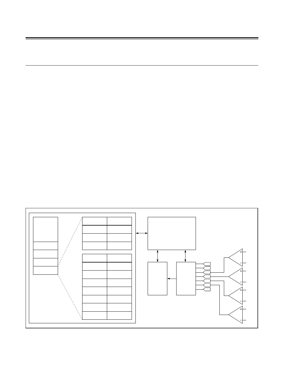
The MAXQ8913 provides a 12-bit, successive approximation analog-to-digital converter (ADC) with an integrated ana-
log multiplexer. The ADC can perform either single-ended conversions from one of six external input channels (and an
additional channel reserved for an internal temperature sensor) or differential conversions from one of three external
channel pairs. The voltage reference used for each conversion can be selected from an internal precision bandgap
reference, an external reference, or the AVDD analog power supply.
19.1 Analog-to-Digital Converter Features
• 12-bit single-ended conversion with up to seven analog channel inputs (six external inputs and one temp sensor)
• 12-bit differential conversion with up to three analog channel pair inputs (each differential pair takes the place of two
single-ended channel inputs)
• Autoscan feature performs up to eight conversions in sequence automatically without CPU intervention
• Conversion sequence can be performed once (single conversion mode) or repeatedly (continuous conversion mode)
• Up to 16 sample words can be stored in a dedicated data buffer until the processor is ready to retrieve them
• Selectable clock divider runs the ADC from a divide by 1, divide by 2, divide by 4, or divide by 8 of the system clock
• Sample acquisition time can optionally be extended on a per-conversion basis
• Data results can be left-aligned or right-aligned on a per-conversion basis
• Converter reference is switchable among AVDD, internal reference, and external reference
• Optional power-management mode shuts the ADC off between conversions to save power
• Configurable data available interrupt signals the CPU following each conversion, each sequence, or after every 12
or 16 samples
• Four uncommitted op amps whose outputs can optionally be used as inputs for channels AIN2, AIN3, AIN4, and AIN5
Figure 19-1. ADC Block Diagram
CPU
INTERFACE
ADC
SEQUENCER
12-BIT
SAR ADC
ADCN
ADST
ADADDR
ADDATA
ADCFG[0]
ADCFG[1]
ADCFG[2]
ADCFG[3]
ADCFG[4]
ADCFG[5]
ADCFG[6]
ADCFG[7]
ADBUF[0]
ADBUF[8]
ADBUF[1]
ADBUF[9]
ADBUF[2]
ADBUF[10]
ADBUF[3]
ADBUF[11]
ADBUF[4]
ADBUF[12]
ADBUF[5]
ADBUF[13]
ADBUF[6]
ADBUF[14]
ADBUF[7]
ADBUF[15]
ANALOG
MULTIPLEXER
AIN0
AIN1
AIN6
(TEMP SENSOR)
INA+
INA-
INB+
INB-
INC+
INC-
IND+
IND-
Maxim Integrated