1 port 0 direction register (pd0, m0[10h]), 2 port 1 direction register (pd1, m0[11h]), 3 port 0 input disable register (pid0, m0[0dh]) – Maxim Integrated MAXQ Family Users Guide: MAXQ8913 Supplement User Manual
Page 35: 3 port 0 input disable register (pid0, m0[0dh]) -3, Maxq family user’s guide: maxq8913 supplement
MAXQ Family User’s Guide:
MAXQ8913 Supplement
6-3
6.1 GPIO and External Interrupt Register Descriptions
The following peripheral registers are used to control the general-purpose I/O and external interrupt features specific
to the MAXQ8913. Addresses of registers are given as “Mx[yy],” where x is the module number (from 0 to 15 decimal)
and yy is the register index (from 00h to 1Fh hexadecimal). Fields in the bit definition tables are defined as follows:
• Name: Symbolic names of bits or bit fields in this register.
• Reset: The value of each bit in this register following a standard reset. If this field reads “unchanged,” the given bit
is unaffected by standard reset. If this field reads “s,” the given bit does not have a fixed 0 or 1 reset value because
its value is determined by another internal state or external condition.
• POR: If present this field defines the value of each bit in this register following a power-on reset (as opposed to a
standard reset). Some bits are unaffected by standard resets and are set/cleared by POR only.
• Access: Bits can be read-only (r) or read/write (rw). Any special restrictions or conditions that could apply when
reading or writing this bit are detailed in the bit description.
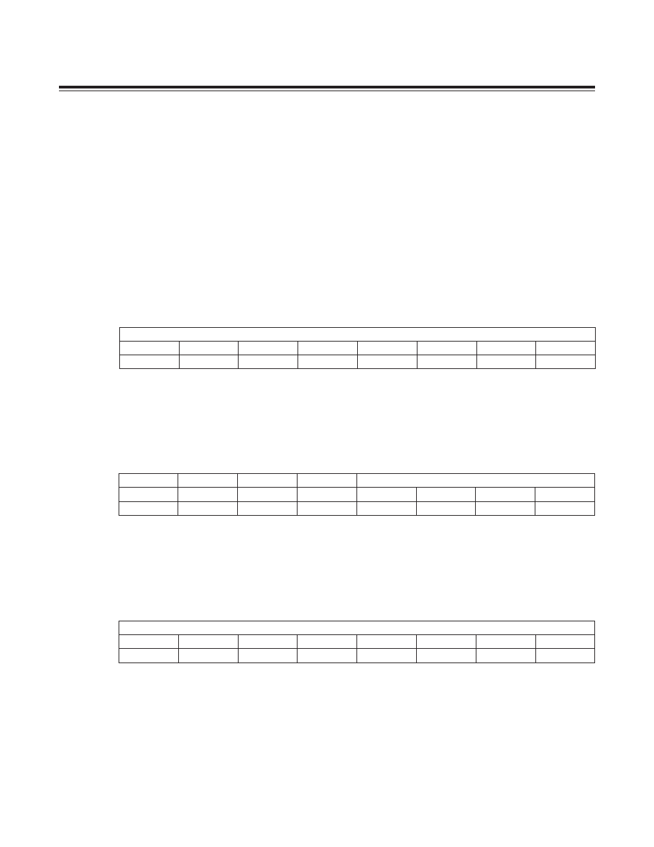
6.1.1 Port 0 Direction Register (PD0, M0[10h])
Each of the bits in this register controls the input/output direction of a port pin (P0.0 to P0.7) as follows:
0 = The port pin is in input mode, either with a weak pullup (if PO = 1) or three-stated (if PO = 0).
1 = The port pin is in output mode, with the output level to drive given by PO.
6.1.2 Port 1 Direction Register (PD1, M0[11h])
Each of the bits in this register controls the input/output direction of a port pin (P1.0 to P1.3) as follows:
0 = The port pin is in input mode, either with a weak pullup (if PO = 1) or three-stated (if PO = 0).
1 = The port pin is in output mode, with the output level to drive given by PO.
6.1.3 Port 0 Input Disable Register (PID0, M0[0Dh])
Each of the bits in this register controls the Schmitt trigger enable of a port pin (P0.0 to P0.7) as follows:
0 = The input Schmitt trigger is enabled; the port pin operates normally.
1 = The input Schmitt trigger is disabled; the port pin cannot be used for input.
Bit #
7
6
5
4
3
2
1
0
Name
PD0
Reset
0
0
0
0
0
0
0
0
Access
rw
rw
rw
rw
rw
rw
rw
rw
Bit #
7
6
5
4
3
2
1
0
Name
—
—
—
—
PD1
Reset
0
0
0
0
0
0
0
0
Access
rw
rw
rw
rw
rw
rw
rw
rw
Bit #
7
6
5
4
3
2
1
0
Name
PID0
Reset
0
0
0
0
0
0
0
0
Access
rw
rw
rw
rw
rw
rw
rw
rw
Maxim Integrated