1 dac 1 output register (dac1out, m3[02h]), 2 dac 2 output register (dac2out, m3[03h]), Maxq family user’s guide: maxq8913 supplement – Maxim Integrated MAXQ Family Users Guide: MAXQ8913 Supplement User Manual
Page 74
MAXQ Family User’s Guide:
MAXQ8913 Supplement
20-2
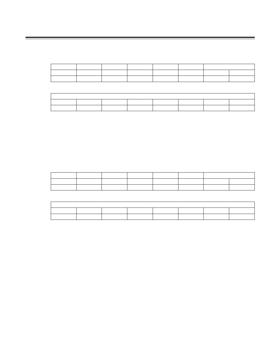
20.2.1 DAC 1 Output Register (DAC1OUT, M3[02h])
Bits 15:10: Reserved
Bits 9:0: DAC 1 Output Value. Bits 9:0 in this register set the voltage output value for the DAC1 channel between zero
(DAC1OUT[9:0] = 0000000000b) and full scale (DAC1OUT[9:0] = 1111111111b). For this register value to be effective,
one or both of the following two register bits in DACEN must be set.
• If DACEN.0 (DACEN1) is set to 1, the DAC1OUT value is output to differential pins RIN+/RIN-.
• If DACEN.4 (DACOUT1) is set to 1, the DAC1OUT value is output to pin DAC1.
20.2.2 DAC 2 Output Register (DAC2OUT, M3[03h])
Bits 15:10: Reserved
Bits 9:0: DAC 2 Output Value. Bits 9:0 in this register set the voltage output value for the DAC2 channel between
zero (if DAC2OUT[9:0] = 0000000000b) and full scale (DAC2OUT[9:0] = 1111111111b). For this register value to be
effective, one or both of the following two register bits in DACEN must be set.
• If DACEN.1 (DACEN2) is set to 1, the DAC2OUT value is output to differential pins LIN+/LIN-.
• If DACEN.5 (DACOUT2) is set to 1, the DAC2OUT value is output to pin DAC2.
Bit #
15
14
13
12
11
10
9
8
Name
—
—
—
—
—
—
DAC1OUT
Reset
0
0
0
0
0
0
0
0
Access
r
r
r
r
r
r
rw
rw
Bit #
7
6
5
4
3
2
1
0
Name
DAC1OUT
Reset
0
0
0
0
0
0
0
0
Access
rw
rw
rw
rw
rw
rw
rw
rw
Bit #
15
14
13
12
11
10
9
8
Name
—
—
—
—
—
—
DAC2OUT
Reset
0
0
0
0
0
0
0
0
Access
r
r
r
r
r
r
rw
rw
Bit #
7
6
5
4
3
2
1
0
Name
DAC2OUT
Reset
0
0
0
0
0
0
0
0
Access
rw
rw
rw
rw
rw
rw
rw
rw
Maxim Integrated