1 dac overview, 2 dac control register descriptions, Maxq family user’s guide: maxq8913 supplement – Maxim Integrated MAXQ Family Users Guide: MAXQ8913 Supplement User Manual
Page 73
MAXQ Family User’s Guide:
MAXQ8913 Supplement
20-1
SECTION 20: DIGITAL-TO-ANALOG CONVERTERS (SPECIFIC TO
MAXQ8913)
20.1 DAC Overview
The MAXQ8913 provides six independent digital-to-analog converter (DAC) channels. Four of these DAC channels
produce voltage outputs, while the other two channels act as programmable current sinks.
The DAC module on the MAXQ8913 provides the following features:
• Two 10-bit (DAC1 and DAC2) voltage output channels that can be used to generate either single-ended (DAC1/
DAC2) or differential (RIN/LIN) voltages.
• Two 8-bit (DAC3 and DAC4) voltage output channels that generate single-ended voltage outputs only.
• Two 8-bit (SINK1 and SINK2) programmable current sinks.
Table 20-1 lists the control registers dedicated to the DAC channels. Note that all DAC pins are dedicated, so none of
them are multiplexed with GPIO port pins.
20.2 DAC Control Register Descriptions
The following peripheral registers are used to control the DAC functions.
Addresses of registers are given as “Mx[yy],”
where x is the module number (from 0 to 15 decimal) and yy is the register index (from 00h to 1Fh hexadecimal). Fields
in the bit definition tables are defined as follows:
• Name: Symbolic names of bits or bit fields in this register.
• Reset: The value of each bit in this register following a standard reset. If this field reads “unchanged,” the given bit
is unaffected by standard reset. If this field reads “s,” the given bit does not have a fixed 0 or 1 reset value because
its value is determined by another internal state or external condition.
• POR: If present this field defines the value of each bit in this register following a power-on reset (as opposed to a
standard reset). Some bits are unaffected by standard resets and are set/cleared by POR only.
• Access: Bits can be read-only (r) or read/write (rw). Any special restrictions or conditions that could apply when
reading or writing this bit are detailed in the bit description.
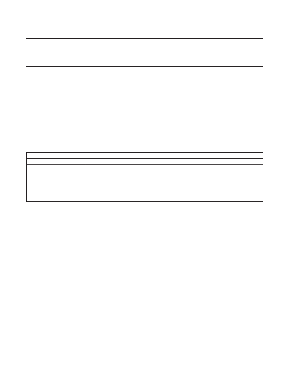
Table 20-1. DAC Control Registers
REGISTER
ADDRESS
FUNCTION
DAC1OUT
M3[02h]
DAC 1 Output Register. Sets the 10-bit voltage output value for DAC channel 1.
DAC2OUT
M3[03h]
DAC 2 Output Register. Sets the 10-bit voltage output value for DAC channel 2.
DAC3OUT
M3[04h]
DAC 3 Output Register. Sets the 8-bit voltage output value for DAC channel 3.
DAC4OUT
M3[05h]
DAC 4 Output Register. Sets the 8-bit voltage output value for DAC channel 4.
ISINKCN
M3[07h]
Current Sink Control Register. Enables/disables and sets the 8-bit current sink capability for
both current sink channels (SINK1 and SINK2).
DACEN
M3[0Bh]
DAC Output Enable Register. Enables/disables the outputs for the four voltage DAC channels.
Maxim Integrated