4 port 0 output register (po0, m0[00h]), 5 port 1 output register (po1, m0[01h]), 6 port 0 input register (pi0, m0[08h]) – Maxim Integrated MAXQ Family Users Guide: MAXQ8913 Supplement User Manual
Page 36: 7 port 1 input register (pi1, m0[09h]), Maxq family user’s guide: maxq8913 supplement
MAXQ Family User’s Guide:
MAXQ8913 Supplement
6-4
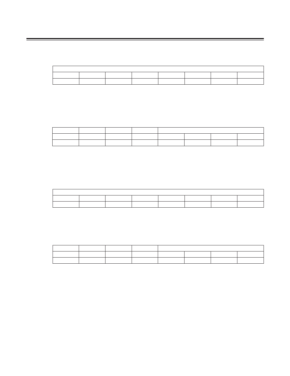
6.1.4 Port 0 Output Register (PO0, M0[00h])
This register stores the data that is output on any of the pins of port 0 that have been defined as output pins. If the port
pins are in input mode, this register controls the weak pullup for each pin. Changing the data direction of any pins for
this port (through register PD0) does not affect the value in this register.
6.1.5 Port 1 Output Register (PO1, M0[01h])
This register stores the data that is output on any of the pins of port 1 that have been defined as output pins. If the port
pins are in input mode, this register controls the weak pullup for each pin. Changing the data direction of any pins for
this port (through register PD1) does not affect the value in this register.
6.1.6 Port 0 Input Register (PI0, M0[08h])
Each of the read-only bits in this register reflects the logic state present at the corresponding port pin, unless the
Schmitt trigger for that pin has been disabled by setting PID0.x to 1.
6.1.7 Port 1 Input Register (PI1, M0[09h])
Each of the read-only bits in this register reflects the logic state present at the corresponding port pin.
Bit #
7
6
5
4
3
2
1
0
Name
PO0
Reset
1
1
1
1
1
1
1
1
Access
rw
rw
rw
rw
rw
rw
rw
rw
Bit #
7
6
5
4
3
2
1
0
Name
—
—
—
—
PO1
Reset
0
0
0
0
1
1
1
1
Access
r
r
r
r
rw
rw
rw
rw
Bit #
7
6
5
4
3
2
1
0
Name
PI0
Reset
s
s
s
s
s
s
s
s
Access
r
r
r
r
r
r
r
r
Bit #
7
6
5
4
3
2
1
0
Name
—
—
—
—
PI1
Reset
0
0
0
0
s
s
s
s
Access
r
r
r
r
r
r
r
r
Maxim Integrated