1 spi input/output pins and control registers, 2 spi code examples, 1 spi example 1: transmitting data in master mode – Maxim Integrated MAXQ Family Users Guide: MAXQ8913 Supplement User Manual
Page 46: Maxq family user’s guide: maxq8913 supplement
MAXQ Family User’s Guide:
MAXQ8913 Supplement
11-1
ADDENDUM TO SECTION 11: SERIAL PERIPHERAL INTERFACE
(SPI) MODULE
The MAXQ8913 provides a serial peripheral interface (SPI) module, which operates as described in the MAXQ Family
User’s Guide with the following additions:
• The maximum clock rate when operating in slave mode is the system clock divided by 4.
• The SPI configuration register (SPICF) contains an additional bit, slave active select (SAS, SPICF.6). This bit allows
the sense of the slave-select input to be changed from active low (SAS = 0, default) to active high (SAS = 1).
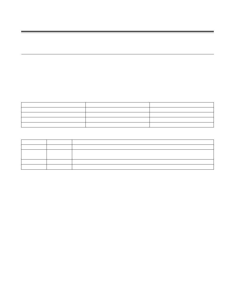
11.1 SPI Input/Output Pins and Control Registers
Table 11-1. SPI Input and Output Pins
Table 11-2. SPI Control Registers
11.2 SPI Code Examples
11.2.1 SPI Example 1: Transmitting Data in Master Mode
move PD5.2, #1
; Chip select for slave device
move PO5.2, #1
; Start high
move SPICN, #03h
; Enable SPI in master mode
move SPICF, #00h
; Sample data at clock rising edge, 8 bit character
move SPICK, #63
; SPI clock = sysclk/128
move PO5.2, #0
; Drive chip select low
move SPIB, #12h
; Transmit byte
call waitXfer
move SPIB, #34h
; Transmit byte
call waitXfer
move PO5.2, #1
; Release chip select
....
waitXfer:
move C, SPICN.6
; Wait for transfer to complete
jump NC, waitXfer
move SPICN.6, #0
; Clear transfer flag
ret
SPI INTERFACE FUNCTION
PIN
MULTIPLEXED WITH GPIO
SSEL: Slave Select
N8
P0.4
SCLK: Slave Clock
M7
P0.5
MOSI: Master Out-Slave In
L6
P0.6
MISO: Master In-Slave Out
K5
P0,7
REGISTER
ADDRESS
FUNCTION
SPICN
M1[02h]
SPI Control Register. Enable, master/slave-mode select, and status and interrupt flags.
SPICF
M1[0Ah]
SPI Configuration Register. Clock polarity/phase, character length, interrupt enable, SSEL
active-high/low mode select (SAS).
SPICK
M1[0Bh]
SPI Clock Register. Master baud rate = 0.5 x Sysclk/(SPICK + 1).
SPIB
M1[03h]
SPI Data Buffer. Writes go to the SPI write buffer; reads come from the SPI read buffer.
Maxim Integrated