Maxim Integrated MAXQ Family Users Guide: MAXQ2000 Supplement User Manual
Maxim Integrated Hardware
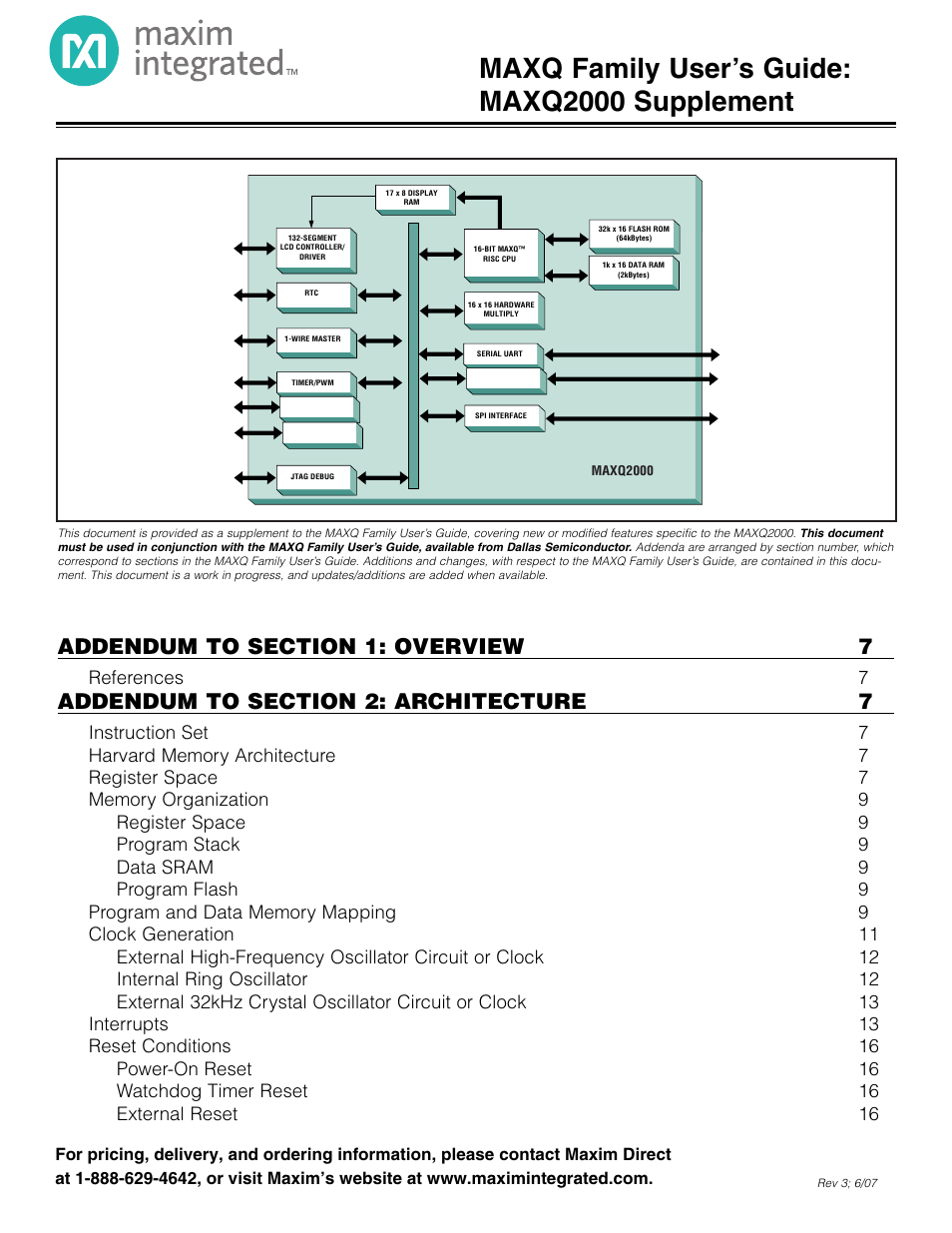
Table of contents
Document Outline
- Table of Contents
- List of Figures
- List of Tables
- Addendum to Section 1: Overview
- Addendum to Section 2: Architecture
- Instruction Set
- Harvard Memory Architecture
- Register Space
- Figure 1. MAXQ2000 System and Peripheral Register Map
- Memory Organization
- Program and Data Memory Mapping
- Figure 2. Memory Map When Executing from Application Flash/ROM
- Figure 3. Memory Map When Executing from Utility ROM
- Figure 4: Memory Map When Executing from Data SRAM
- Clock Generation
- Figure 5. MAXQ2000 Clock Sources
- Table 1. System Clock Generation and Control Registers
- Interrupts
- Table 2. MAXQ2000 Interrupt Sources and Control Bits
- Reset Conditions
- Figure 6. MAXQ2000 Power-On Reset
- Figure 7. MAXQ2000 External Reset
- Table 3. System Power Management Registers
- Power Management Features
- Addendum to Section 3: Programming
- Addendum to Section 4: System Register Descriptions
- Addendum to Section 5: Peripheral Register Modules
- Addendum to Section 6: General-Purpose I/O Module (GPIO and External Interrupts)
- Addendum to Section 7: Timer/Counter 0 Module
- Addendum to Section 8: Timer/Counter 1 Module
- Addendum to Section 9: Timer/Counter 2 Module
- Addendum to Section 10: Serial I/O Module
- Addendum to Section 11: Serial Peripheral Interface (SPI) Module
- Addendum to Section 12: Hardware Multiplier Module
- Addendum to Section 13: 1-Wire Bus Master
- Addendum to Section 14: Real-Time Clock Module
- Addendum to Section 15: Test Access Port (TAP)
- Addendum to Section 16: In-Circuit Debug Mode
- Addendum to Section 17: In-System Programming (JTAG)
- Bootload Protocol
- Table 26. Bootloader Status Codes
- Family 0 Commands (Not Password Protected)
- Table 27. Bootloader Status Flags
- Family 1 Commands: Load Variable Length (Password Protected)
- Family 2 Commands: Dump Variable Length (Password Protected)
- Family 3 Commands: CRC Variable Length (Password Protected)
- Family 4 Commands: Verify Variable Length (Password Protected)
- Family 5 Commands: Load and Verify Variable Length (Password Protected)
- Family 6 Commands: Erase Variable Length (Password Protected)
- Family E Commands: Erase Fixed Length (Password Protected)
- Addendum to Section 18: MAXQ Family Instruction Set Summary
- LCD Controller (Specific to MAXQ200)
- LCD Controller Features
- Figure 8. LCD Controller Block Diagram
- Table 28. PCFn Bit Functions for 68-Pin Package
- Table 29. PCFn Bit Functions for 56-Pin Package
- LCD Controller Operation Modes
- LCD Drive Voltages
- Figure 9. LCD Drive Voltage Generation
- Selecting the LCD Mode
- Table 30. LCD Display Modes
- Segment Pin Configuration
- LCD Internal Adjustable Contrast Resistor
- Figure 10. LCD Internal and External Display Contrast Adjustment
- LCD Frame Frequency
- Table 31. LCD Frame Frequencies (Hz)
- LCD Display Memory
- Table 32. LCD Display Memory Map (Static, 56-Pin Package)
- Table 33. LCD Display Memory Map (1/2 Duty, 56-Pin Package)
- Table 34. LCD Display Memory Map (1/3 Duty, 56-Pin Package)
- Table 35. LCD Display Memory Map (1/4 Duty, 56-Pin Package)
- Table 36. LCD Display Memory Map (Static, 68-Pin Package)
- Table 37. LCD Display Memory Map (1/2 Duty, 68-Pin Package)
- Table 38. LCD Display Memory Map (Static, 68-Pin Package)
- Table 39. LCD Display Memory Map (1/4 Duty, 68-Pin Package)
- Display Waveform Generation
- LCD Controller Static Drive Example
- Figure 11. Sample 7-Segment LCD Display
- Figure 12. Static Drive Example Display Connection
- Table 40. Static Drive Example Common Signal Selection
- Table 41. Static Drive Example Register Content
- Figure 13. Static Drive Example Waveform Timing
- LCD Controller 1/2 Duty Cycle Drive Example
- Figure 14. 1/2 Duty Drive Example Display Connection
- Table 42. 1/2 Duty Drive Example Common Signal Selection
- Table 43. 1/2 Duty Drive Example Register Content
- Figure 15. 1/2 Duty Drive Example Waveform Timing
- LCD Controller 1/3 Duty Cycle Drive Example
- Figure 16. 1/3 Drive Example Display Connection
- Table 44. 1/3 Duty Drive Example Common Signal Selection
- Table 45. 1/3 Duty Drive Example Register Content
- Figure 17. 1/3 Duty Drive Example Waveform Timing
- LCD Controller 1/4 Duty Cycle Drive Example
- Figure 18. 1/4 Duty Drive Example Display Connection
- Table 46. 1/4 Duty Drive Example Common Signal Selection
- Table 47. 1/4 Duty Drive Example Register Content
- Figure 19. 1/4 Duty Drive Example Waveform Timing
- LCD Controller Example: Initializing the LCD Controller
- Utility ROM (Specific to MAXQ2000)
- Revision History