Maxq family user’s guide: maxq2000 supplement – Maxim Integrated MAXQ Family Users Guide: MAXQ2000 Supplement User Manual
Page 37
The following peripheral registers control the general-purpose I/O and external interrupt features specific to the MAXQ2000.
Register Name:
PO0
Register Description:
Port 0 Output Register
Register Address:
M0[00h]
Bits 0 to 7: (PO0.0 to PO0.7) Port 0 Output. This register stores the data that will be output on any of the pins of Port 0 that have been
defined as output pins. If the port pins are in input mode, this register controls the weak pullup for each pin. Changing the data direc-
tion of any pins for this port (through register PD0) will not affect the value in this register.
Register Name:
PO1
Register Description:
Port 1 Output Register
Register Address:
M0[01h]
Bits 0 to 7: (PO1.0 to PO1.7) Port 1 Output. This register stores the data that will be output on any of the pins of Port 1 that have been
defined as output pins. If the port pins are in input mode, this register controls the weak pullup for each pin. Changing the data direc-
tion of any pins for this port (through register PD1) will not affect the value in this register.
Register Name:
PO2
Register Description:
Port 2 Output Register
Register Address:
M0[02h]
Bits 0 to 7: (PO2.0 to PO2.7) Port 2 Output. This register stores the data that will be output on any of the pins of Port 2 that have been
defined as output pins. If the port pins are in input mode, this register controls the weak pullup for each pin. Changing the data direc-
tion of any pins for this port (through register PD2) will not affect the value in this register.
MAXQ Family User’s Guide:
MAXQ2000 Supplement
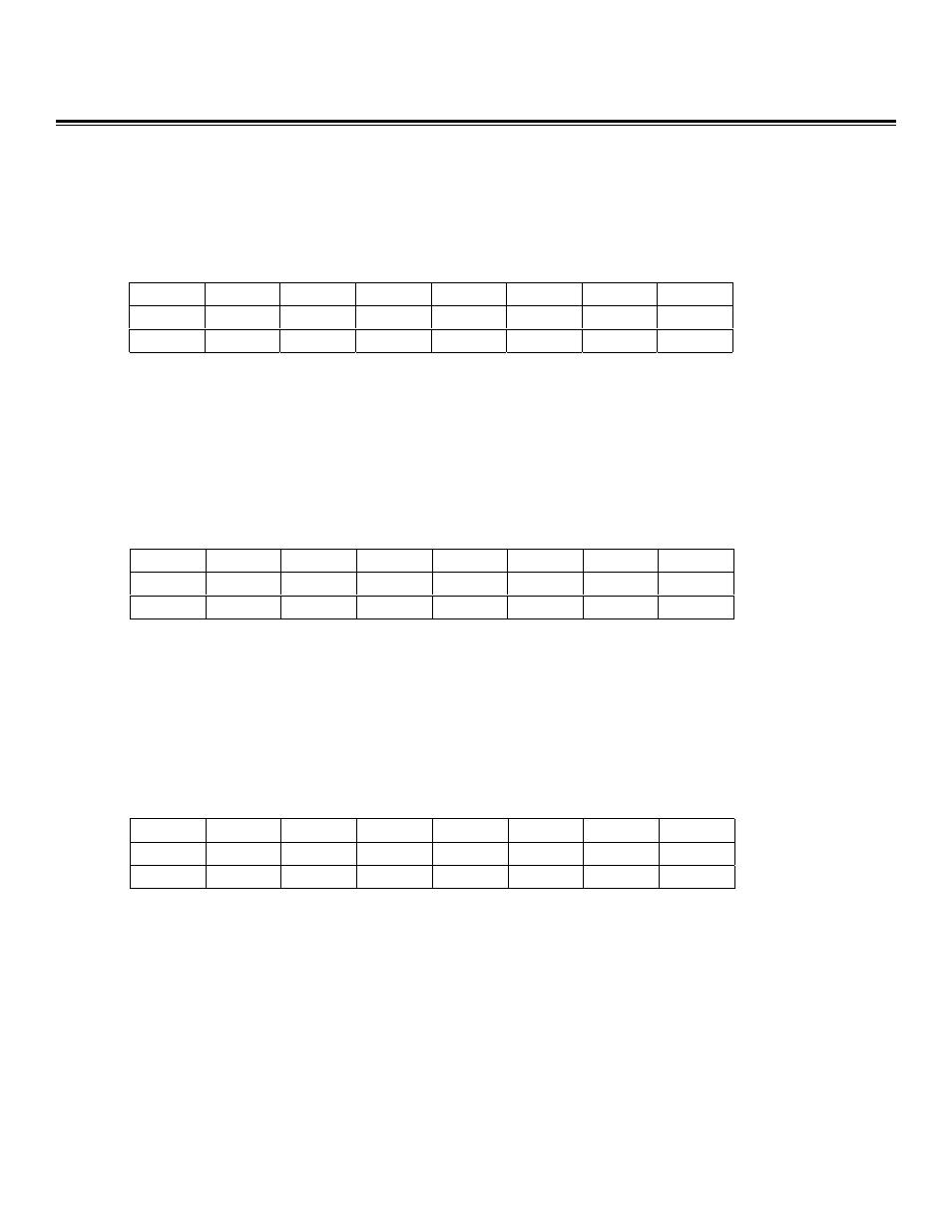
Bit #
7
6
5
4
3
2
1
0
Name
PO0.7
PO0.6
PO0.5
PO0.4
PO0.3
PO0.2
PO0.1
PO0.0
Reset
1
1
1
1
1
1
1
1
Access
r/w
r/w
r/w
r/w
r/w
r/w
r/w
r/w
Bit #
7
6
5
4
3
2
1
0
Name
PO1.7
PO1.6
PO1.5
PO1.4
PO1.3
PO1.2
PO1.1
PO1.0
Reset
1
1
1
1
1
1
1
1
Access
r/w
r/w
r/w
r/w
r/w
r/w
r/w
r/w
Bit #
7
6
5
4
3
2
1
0
Name
PO2.7
PO2.6
PO2.5
PO2.4
PO2.3
PO2.2
PO2.1
PO2.0
Reset
1
1
1
1
1
1
1
1
Access
r/w
r/w
r/w
r/w
r/w
r/w
r/w
r/w
Maxim Integrated
37