Maxq family user’s guide: maxq2000 supplement – Maxim Integrated MAXQ Family Users Guide: MAXQ2000 Supplement User Manual
Page 40
MAXQ Family User’s Guide:
MAXQ2000 Supplement
Register Name:
PI3
Register Description:
Port 3 Input Register
Register Address:
M0[0Bh]
Each of the read-only bits in this register reflects the logic state present at the corresponding port pin.
Register Name:
EIES0
Register Description:
External Interrupt Edge Select 0 Register
Register Address:
M0[0Ch]
Each bit in this register controls the edge select mode for an external interrupt, as follows:
0 = The external interrupt will trigger on a rising (positive) edge.
1 = The external interrupt will trigger on a negative (falling) edge.
Bit 0: (EIES0.0) Edge Select for External Interrupt 0 (IT0)
Bit 1: (EIES0.1) Edge Select for External Interrupt 1 (IT1)
Bit 2: (EIES0.2) Edge Select for External Interrupt 2 (IT2)
Bit 3: (EIES0.3) Edge Select for External Interrupt 3 (IT3)
Bit 4: (EIES0.4) Edge Select for External Interrupt 4 (IT4)
Bit 5: (EIES0.5) Edge Select for External Interrupt 5 (IT5)
Bit 6: (EIES0.6) Edge Select for External Interrupt 6 (IT6)
Bit 7: (EIES0.7) Edge Select for External Interrupt 7 (IT7)
Register Name:
PD0
Register Description:
Port 0 Direction Register
Register Address:
M0[10h]
Each of the bits in this register controls the input/output direction of a port pin (P0.0 to P0.7), as follows.
0 = The port pin is in input mode, either with a weak pullup (if PO = 1) or tri-stated (if PO = 0).
1 = The port pin is in output mode, with the output level to drive given by PO.
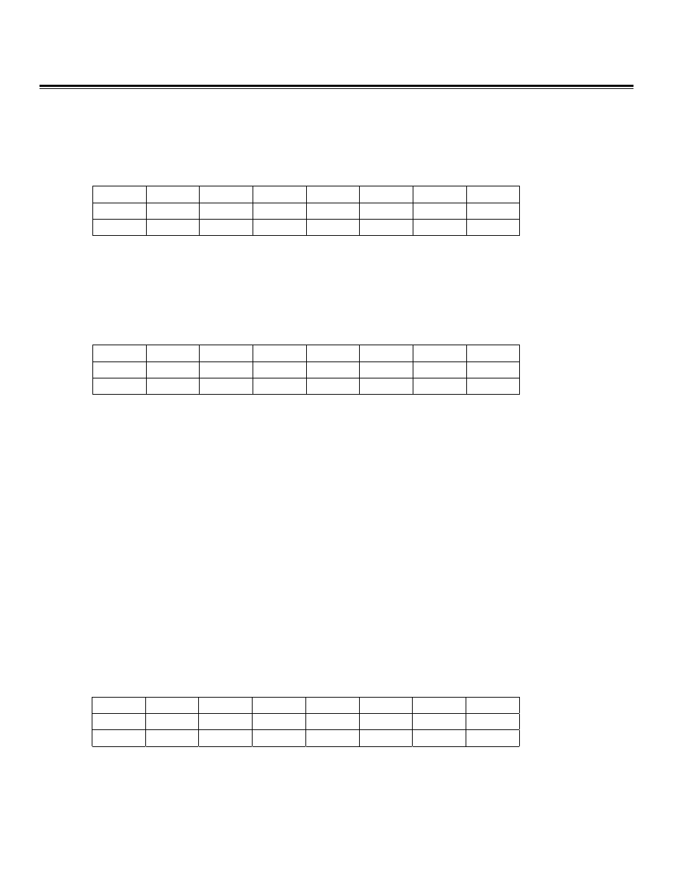
Bit #
7
6
5
4
3
2
1
0
Name
PI3.7
PI3.6
PI3.5
PI3.4
PI3.3
PI3.2
PI3.1
PI3.0
Reset
s
s
s
s
s
s
s
s
Access
r
r
r
r
r
r
r
r
Bit #
7
6
5
4
3
2
1
0
Name
IT7
IT6
IT5
IT4
IT3
IT2
IT1
IT0
Reset
0
0
0
0
0
0
0
0
Access
r/w
r/w
r/w
r/w
r/w
r/w
r/w
r/w
Bit #
7
6
5
4
3
2
1
0
Name
PD0.7
PD0.6
PD0.5
PD0.4
PD0.3
PD0.2
PD0.1
PD0.0
Reset
0
0
0
0
0
0
0
0
Access
r/w
r/w
r/w
r/w
r/w
r/w
r/w
r/w
Maxim Integrated
40