Maxq family user’s guide: maxq2000 supplement – Maxim Integrated MAXQ Family Users Guide: MAXQ2000 Supplement User Manual
Page 41
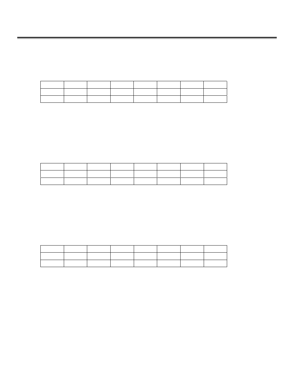
Register Name:
PD1
Register Description:
Port 1 Direction Register
Register Address:
M0[11h]
Each of the bits in this register controls the input/output direction of a port pin (P1.0 to P1.7), as follows.
0 = The port pin is in input mode, either with a weak pullup (if PO = 1) or tri-stated (if PO = 0).
1 = The port pin is in output mode, with the output level to drive given by PO.
Register Name:
PD2
Register Description:
Port 2 Direction Register
Register Address:
M0[12h]
Each of the bits in this register controls the input/output direction of a port pin (P2.0 to P2.7), as follows.
0 = The port pin is in input mode, either with a weak pullup (if PO = 1) or tri-stated (if PO = 0).
1 = The port pin is in output mode, with the output level to drive given by PO.
Register Name:
PD3
Register Description:
Port 3 Direction Register
Register Address:
M0[13h]
Each of the bits in this register controls the input/output direction of a port pin (P3.0 to P3.7), as follows.
0 = The port pin is in input mode, either with a weak pullup (if PO = 1) or tri-stated (if PO = 0).
1 = The port pin is in output mode, with the output level to drive given by PO.
MAXQ Family User’s Guide:
MAXQ2000 Supplement
Bit #
7
6
5
4
3
2
1
0
Name
PD1.7
PD1.6
PD1.5
PD1.4
PD1.3
PD1.2
PD1.1
PD1.0
Reset
0
0
0
0
0
0
0
0
Access
r/w
r/w
r/w
r/w
r/w
r/w
r/w
r/w
Bit #
7
6
5
4
3
2
1
0
Name
PD2.7
PD2.6
PD2.5
PD2.4
PD2.3
PD2.2
PD2.1
PD2.0
Reset
0
0
0
0
0
0
0
0
Access
r/w
r/w
r/w
r/w
r/w
r/w
r/w
r/w
Bit #
7
6
5
4
3
2
1
0
Name
PD3.7
PD3.6
PD3.5
PD3.4
PD3.3
PD3.2
PD3.1
PD3.0
Reset
0
0
0
0
0
0
0
0
Access
r/w
r/w
r/w
r/w
r/w
r/w
r/w
r/w
Maxim Integrated
41