Maxim Integrated MAXQ Family Users Guide: MAXQ2000 Supplement User Manual
Maxim Integrated Hardware

Pin Configurations appear at end of data sheet.
Functional Diagrams continued at end of data sheet.
UCSP is a trademark of Maxim Integrated Products, Inc.
For pricing, delivery, and ordering information, please contact Maxim Direct
at 1-888-629-4642, or visit Maxim’s website at www.maximintegrated.com.
MAXQ Family User’s Guide:
MAXQ2000 Supplement
TABLE OF CONTENTS
Rev 3; 6/07
ADDENDUM TO SECTION 1: OVERVIEW
ADDENDUM TO SECTION 2: ARCHITECTURE
Program and Data Memory Mapping
External High-Frequency Oscillator Circuit or Clock
External 32kHz Crystal Oscillator Circuit or Clock
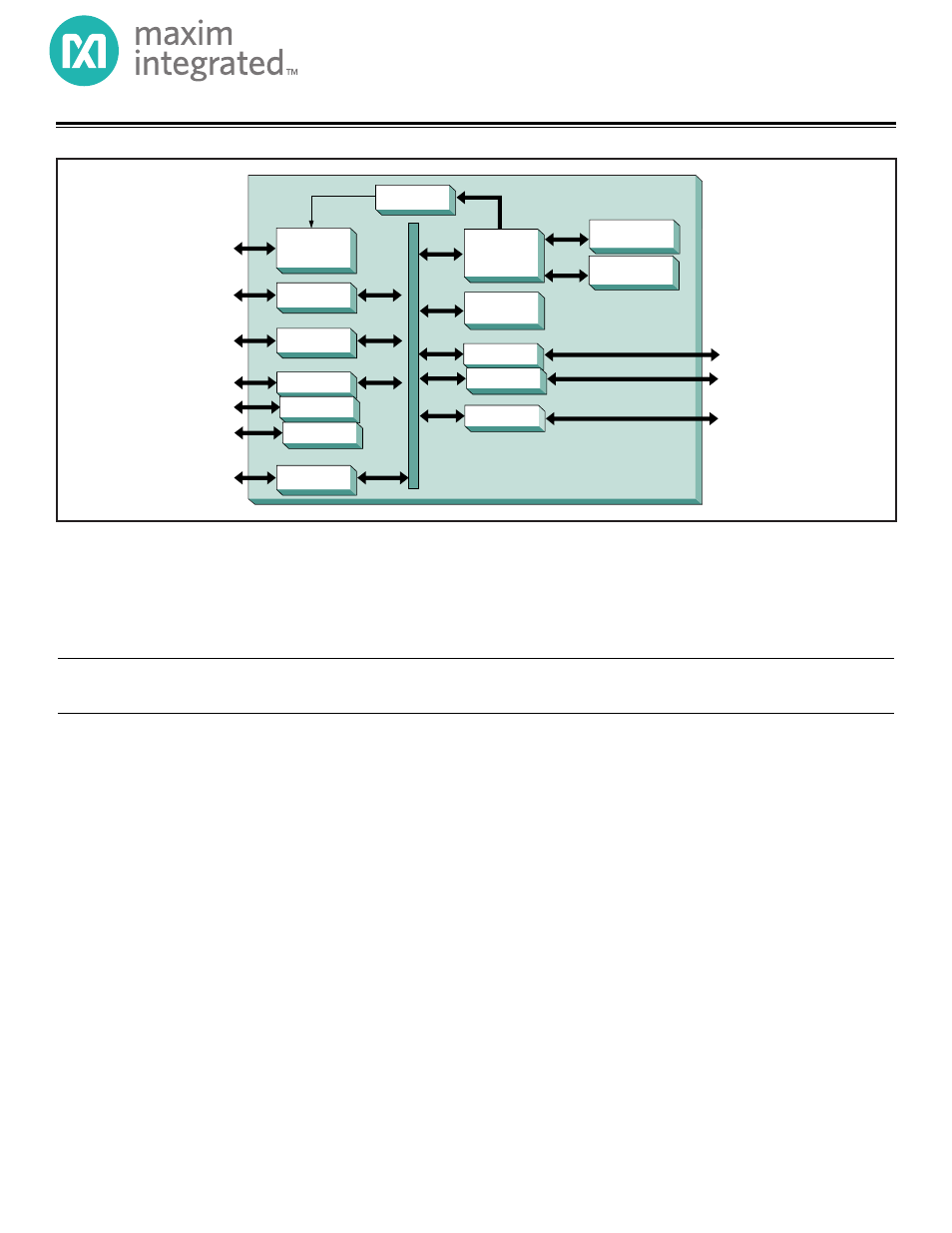
MAXQ2000
132-SEGMENT
LCD CONTROLLER/
DRIVER
RTC
1-WIRE MASTER
TIMER/PWM
16-BIT MAXQ™
RISC CPU
32k x 16 FLASH ROM
(64kBytes)
1k x 16 DATA RAM
(2kBytes)
16 x 16 HARDWARE
MULTIPLY
JTAG DEBUG
SERIAL UART
SPI INTERFACE
17 x 8 DISPLAY
RAM
This document is provided as a supplement to the MAXQ Family User’s Guide, covering new or modified features specific to the MAXQ2000. This document
must be used in conjunction with the MAXQ Family User’s Guide, available from Dallas Semiconductor. Addenda are arranged by section number, which
correspond to sections in the MAXQ Family User’s Guide. Additions and changes, with respect to the MAXQ Family User’s Guide, are contained in this docu-
ment. This document is a work in progress, and updates/additions are added when available.
Document Outline
- Table of Contents
- List of Figures
- List of Tables
- Addendum to Section 1: Overview
- Addendum to Section 2: Architecture
- Instruction Set
- Harvard Memory Architecture
- Register Space
- Figure 1. MAXQ2000 System and Peripheral Register Map
- Memory Organization
- Program and Data Memory Mapping
- Figure 2. Memory Map When Executing from Application Flash/ROM
- Figure 3. Memory Map When Executing from Utility ROM
- Figure 4: Memory Map When Executing from Data SRAM
- Clock Generation
- Figure 5. MAXQ2000 Clock Sources
- Table 1. System Clock Generation and Control Registers
- Interrupts
- Table 2. MAXQ2000 Interrupt Sources and Control Bits
- Reset Conditions
- Figure 6. MAXQ2000 Power-On Reset
- Figure 7. MAXQ2000 External Reset
- Table 3. System Power Management Registers
- Power Management Features
- Addendum to Section 3: Programming
- Addendum to Section 4: System Register Descriptions
- Addendum to Section 5: Peripheral Register Modules
- Addendum to Section 6: General-Purpose I/O Module (GPIO and External Interrupts)
- Addendum to Section 7: Timer/Counter 0 Module
- Addendum to Section 8: Timer/Counter 1 Module
- Addendum to Section 9: Timer/Counter 2 Module
- Addendum to Section 10: Serial I/O Module
- Addendum to Section 11: Serial Peripheral Interface (SPI) Module
- Addendum to Section 12: Hardware Multiplier Module
- Addendum to Section 13: 1-Wire Bus Master
- Addendum to Section 14: Real-Time Clock Module
- Addendum to Section 15: Test Access Port (TAP)
- Addendum to Section 16: In-Circuit Debug Mode
- Addendum to Section 17: In-System Programming (JTAG)
- Bootload Protocol
- Table 26. Bootloader Status Codes
- Family 0 Commands (Not Password Protected)
- Table 27. Bootloader Status Flags
- Family 1 Commands: Load Variable Length (Password Protected)
- Family 2 Commands: Dump Variable Length (Password Protected)
- Family 3 Commands: CRC Variable Length (Password Protected)
- Family 4 Commands: Verify Variable Length (Password Protected)
- Family 5 Commands: Load and Verify Variable Length (Password Protected)
- Family 6 Commands: Erase Variable Length (Password Protected)
- Family E Commands: Erase Fixed Length (Password Protected)
- Addendum to Section 18: MAXQ Family Instruction Set Summary
- LCD Controller (Specific to MAXQ200)
- LCD Controller Features
- Figure 8. LCD Controller Block Diagram
- Table 28. PCFn Bit Functions for 68-Pin Package
- Table 29. PCFn Bit Functions for 56-Pin Package
- LCD Controller Operation Modes
- LCD Drive Voltages
- Figure 9. LCD Drive Voltage Generation
- Selecting the LCD Mode
- Table 30. LCD Display Modes
- Segment Pin Configuration
- LCD Internal Adjustable Contrast Resistor
- Figure 10. LCD Internal and External Display Contrast Adjustment
- LCD Frame Frequency
- Table 31. LCD Frame Frequencies (Hz)
- LCD Display Memory
- Table 32. LCD Display Memory Map (Static, 56-Pin Package)
- Table 33. LCD Display Memory Map (1/2 Duty, 56-Pin Package)
- Table 34. LCD Display Memory Map (1/3 Duty, 56-Pin Package)
- Table 35. LCD Display Memory Map (1/4 Duty, 56-Pin Package)
- Table 36. LCD Display Memory Map (Static, 68-Pin Package)
- Table 37. LCD Display Memory Map (1/2 Duty, 68-Pin Package)
- Table 38. LCD Display Memory Map (Static, 68-Pin Package)
- Table 39. LCD Display Memory Map (1/4 Duty, 68-Pin Package)
- Display Waveform Generation
- LCD Controller Static Drive Example
- Figure 11. Sample 7-Segment LCD Display
- Figure 12. Static Drive Example Display Connection
- Table 40. Static Drive Example Common Signal Selection
- Table 41. Static Drive Example Register Content
- Figure 13. Static Drive Example Waveform Timing
- LCD Controller 1/2 Duty Cycle Drive Example
- Figure 14. 1/2 Duty Drive Example Display Connection
- Table 42. 1/2 Duty Drive Example Common Signal Selection
- Table 43. 1/2 Duty Drive Example Register Content
- Figure 15. 1/2 Duty Drive Example Waveform Timing
- LCD Controller 1/3 Duty Cycle Drive Example
- Figure 16. 1/3 Drive Example Display Connection
- Table 44. 1/3 Duty Drive Example Common Signal Selection
- Table 45. 1/3 Duty Drive Example Register Content
- Figure 17. 1/3 Duty Drive Example Waveform Timing
- LCD Controller 1/4 Duty Cycle Drive Example
- Figure 18. 1/4 Duty Drive Example Display Connection
- Table 46. 1/4 Duty Drive Example Common Signal Selection
- Table 47. 1/4 Duty Drive Example Register Content
- Figure 19. 1/4 Duty Drive Example Waveform Timing
- LCD Controller Example: Initializing the LCD Controller
- Utility ROM (Specific to MAXQ2000)
- Revision History
