Addendum to section 7: timer/counter 0 module, Addendum to section 8: timer/counter 1 module, Addendum to section 9: timer/counter 2 module – Maxim Integrated MAXQ Family Users Guide: MAXQ2000 Supplement User Manual
Page 49: Table 14. type 2 timer/counter control registers, Maxq family user’s guide: maxq2000 supplement, Using the 32khz alternate timer clock source
ADDENDUM TO SECTION 7: TIMER/COUNTER 0 MODULE
The MAXQ2000 does not provide these peripherals. Refer to the MAXQ Family User’s Guide.
ADDENDUM TO SECTION 8: TIMER/COUNTER 1 MODULE
The MAXQ2000 does not provide these peripherals. Refer to the MAXQ Family User’s Guide.
ADDENDUM TO SECTION 9: TIMER/COUNTER 2 MODULE
The MAXQ2000 provides three Type 2 timer/counters (Timer 0, Timer 1, Timer 2), which operate as described in the MAXQ Family
User’s Guide. Table 13 shows the associated pins and Table 14 shows the associated registers for these timer/counters.
Using the 32kHz Alternate Timer Clock Source
The 32kHz clock can be used as an alternate Timer 2 clock source by setting the T2CI bit in that timer’s T2CFG register to 1. Note that
for this to work properly, either the 32kHz crystal oscillator must be enabled (by clearing the X32D/RCNT.14 bit to zero) with a 32kHz
external crystal connected between pins 32KIN and 32KOUT, or the 32kHz clock must be driven directly by an external 32kHz clock
source at 32KIN.
Additionally, because the Timer 2 alternate clock source is sampled by the system clock, for proper operation the system clock must
either be (a) running directly from the 32kHz clock source, or (b) running at a frequency greater than (32kHz x 4).
MAXQ Family User’s Guide:
MAXQ2000 Supplement
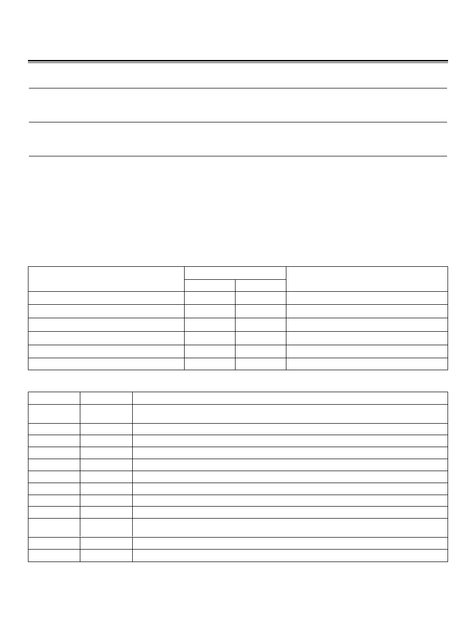
PIN NUMBER
TIMER/COUNTER FUNCTION
68-PIN
56-PIN
MULTIPLEXED WITH PORT PIN
Timer 0 Input/Output—T0 (T2P)
48
39
P6.5
Timer 0 Secondary Output—T0B (T2PB)
47
38
P6.4
Timer 1 Input/Output—T1 (T2P)
44
37
P6.1
Timer 1 Secondary Output—T1B (T2PB)
43
36
P6.0
Timer 2 Input/Output—T2 (T2P)
46
—
P6.2
Timer 2 Secondary Output—T2B (T2PB)
45
—
P6.1
REGISTER
ADDRESS
FUNCTION
T2CFG0
M3[10h]
Timer/Counter 0 (Type 2) Configuration Register. Controls counter/timer select, capture/compare function
select, 8-bit/16-bit mode select, and clock divide modes.
T2CNA0
M3[00h]
Timer/Counter 0 (Type 2) Control Register A. I/O settings, run enables, polarity modes.
T2CNB0
M3[0Ch]
Timer/Counter 0 (Type 2) Control Register B. Contains capture, compare, overflow flags.
T2V0
M3[0Dh]
Timer/Counter 0 (Type 2) Value Register
T2H0
M3[01h]
Timer/Counter 0 (Type 2) Value MSB Register. Provides access to high byte of T2V.
T2R0
M3[0Eh]
Timer/Counter 0 (Type 2) Reload Register
T2RH0
M3[02h]
Timer/Counter 0 (Type 2) Reload MSB Register. Provides access to high byte of T2R.
T2C0
M3[0Fh]
Timer/Counter 0 (Type 2) Capture/Compare Register
T2CH0
M3[03h]
Timer/Counter 0 (Type 2) Capture/Compare MSB Register. Access to high byte of T2C.
T2CFG1
M4[10h]
Timer/Counter 1 (Type 2) Configuration Register. Controls counter/timer select, capture/compare function
select, 8-bit/16-bit mode select, and clock divide modes.
T2CNA1
M4[00h]
Timer/Counter 1 (Type 2) Control Register A. I/O settings, run enables, polarity modes.
T2CNB1
M4[08h]
Timer/Counter 1 (Type 2) Control Register B. Contains capture, compare, overflow flags.
Table 13. Type 2 Timer/Counter Input and Output Pins
Table 14. Type 2 Timer/Counter Control Registers
Maxim Integrated
49