Segment pin configuration, Lcd internal adjustable contrast resistor, Maxq family user’s guide: maxq2000 supplement – Maxim Integrated MAXQ Family Users Guide: MAXQ2000 Supplement User Manual
Page 74
MAXQ Family User’s Guide:
MAXQ2000 Supplement
STATIC DISPLAY
R
R
V
LCD2
V
ADJ
R
V
LCD
V
LCD1
R
ADJ
GNDIO
LRIG = 1
STATIC DISPLAY
R
R
V
LCD2
V
ADJ
R
V
LCD
V
LCD1
R
ADJ
GNDIO
LRIG = 0
R
EXT
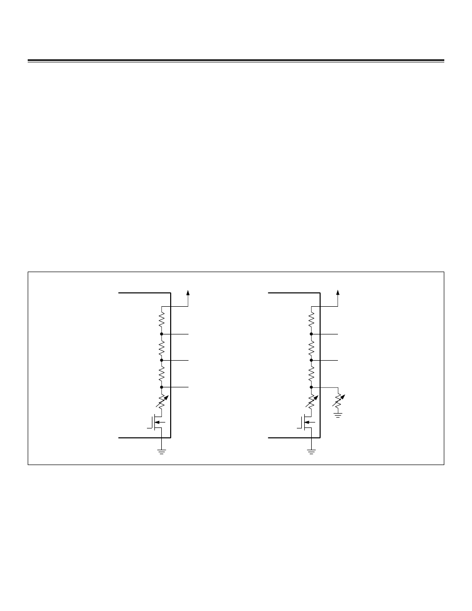
Figure 10. LCD Internal and External Display Contrast Adjustment
Segment Pin Configuration
The PCF[3:0] bits in the LCFG register switch four banks of pins between LCD segment-display mode and general-purpose port-pin
mode. These pins are grouped in banks of four or eight, depending on the package type. Since all of the PCF bits default to 0 on reset,
all pins that share LCD segment and port pin capability act as port pins by default. To enable these pins for LCD segment display, the
PCF bits must be set appropriately and the LCD controller must be in normal operational mode.
Some of the port pins controlled by the PCF bits have external interrupt capability. If the external interrupt function is enabled for any
of these port pins, this function overrides the PCF bit setting for that pin only. The pin remains a port pin (with an external interrupt
enabled) regardless of the function of the other pins in its bank. The other pins in the bank can still be used for LCD segment display.
LCD Internal Adjustable Contrast Resistor
For an LCD segment to be in the OFF state, the V
RMS
voltage between its COM and SEG signals must remain below the threshold volt-
age for that particular LCD display. As the V
RMS
voltage difference increases, the LCD segment remains OFF until the threshold volt-
age is reached, at which point it turns ON. As the V
RMS
difference continues to increase, the contrast of the LCD segment increases
too (the segment becomes darker).
To adjust the visible contrast level for all LCD segments, the internal adjustable resistor R
ADJ
can be varied between 0kΩ and 200kΩ
by setting the bits LRA0 to LRA4 (LCRA.0 to LCRA.4). Changing this value causes the difference among V
LCD
, V
LCD1
, V
LCD2
, and
V
ADJ
to increase or decrease evenly for all four drive voltages.
For the internal resistor R
ADJ
to be used in this manner, the LRIG bit must be set to 1 to connect R
ADJ
to ground internally. If an exter-
nal adjustable resistor is used for the contrast adjustment function, LRIG should be set to 0, and the external resistor R
EXT
should be
connected between V
ADJ
and ground as shown in Figure 10.
Maxim Integrated
74