Table 28. pcfn bit functions for 68-pin package, Table 29. pcfn bit functions for 56-pin package, Maxq family user’s guide: maxq2000 supplement – Maxim Integrated MAXQ Family Users Guide: MAXQ2000 Supplement User Manual
Page 67
The following peripheral registers are used to control the LCD controller.
Register Name:
LCFG
Register Description:
LCD Configuration Register
Register Address:
M2[0Eh]
Bit 0: (LCFG.0) Display Enable (DPE). When the LCD controller is in normal operating mode, this bit controls whether the display reg-
ister data is used to drive the LCD. This bit has no meaning when LCD operation is suspended (OPM = 0).
0 = Disables the LCD display. SEG and COM waveforms are driven to turn all segments OFF.
1 = Drive the LCD display normally.
Bit 1: (LCFG.1) Operation Mode (OPM). This bit determines whether the LCD controller is operating (driving SEG and COM lines) or
suspended (with its clock gated off).
0 = The LCD controller is suspended.
1 = The LCD controller is in normal operating mode.
Bits 2 and 3: (LCFG.2 and LCFG.3) Reserved
Bits 4 to 7: (LCFG.4 to LCFG.7) Segment Pin Configuration (PCF0 to PCF3). Each of these bits controls whether a group of pins
operates as port pin I/O or as LCD segment outputs. The specific pins controlled by each bit depend on the package type, as shown
in Table 28 and Table 29.
MAXQ Family User’s Guide:
MAXQ2000 Supplement
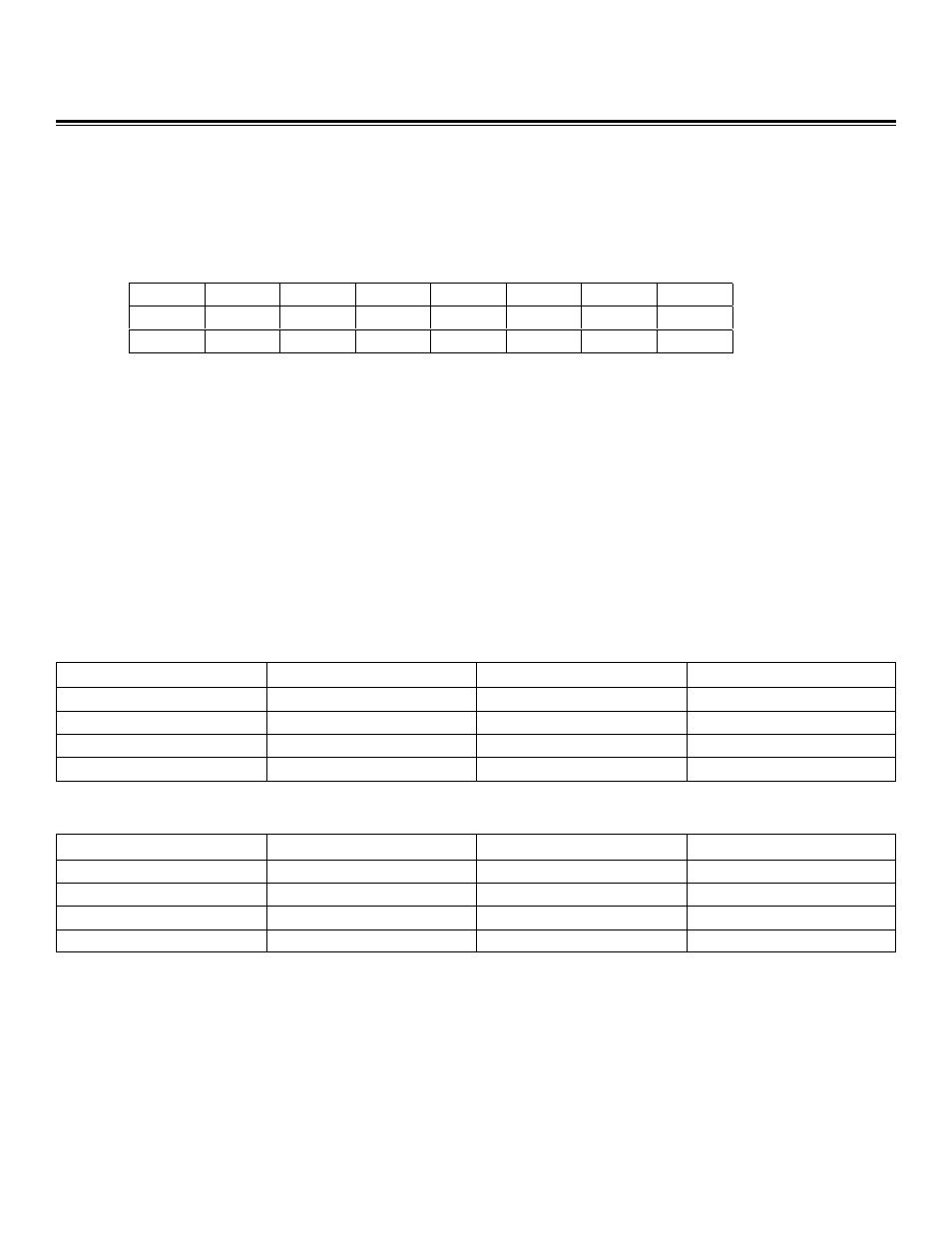
Bit #
7
6
5
4
3
2
1
0
Name
PCF3
PCF2
PCF1
PCF0
—
—
OPM
DPE
Reset
0
0
0
0
0
0
0
0
Access
r/w
r/w
r/w
r/w
r/w
r/w
r/w
r/w
BIT
PINS AFFECTED
FUNCTION WHEN PCFn = 0
FUNCTION WHEN PCFn = 1
PCF0
58 to 65
P0.0 to P0.7
SEG0 to SEG7
PCF1
66 to 68, 1 to 5
P1.0 to P1.7
SEG8 to SEG15
PCF2
6 to 13
P2.0 to P2.7
SEG16 to SEG23
PCF3
14 to 21
P3.0 to P3.7
SEG24 to SEG31
Table 28. PCFn Bit Functions for 68-Pin Package
BIT
PINS AFFECTED
FUNCTION WHEN PCFn = 0
FUNCTION WHEN PCFn = 1
PCF0
49 to 56
P0.0 to P0.7
SEG0 to SEG7
PCF1
1 to 8
P1.0 to P1.7
SEG8 to SEG15
PCF2
9 to 12
P2.4 to P2.7
SEG16 to SEG19
PCF3
13 to 16
P3.4 to P3.7
SEG20 to SEG27
Table 29. PCFn Bit Functions for 56-Pin Package
Maxim Integrated
67