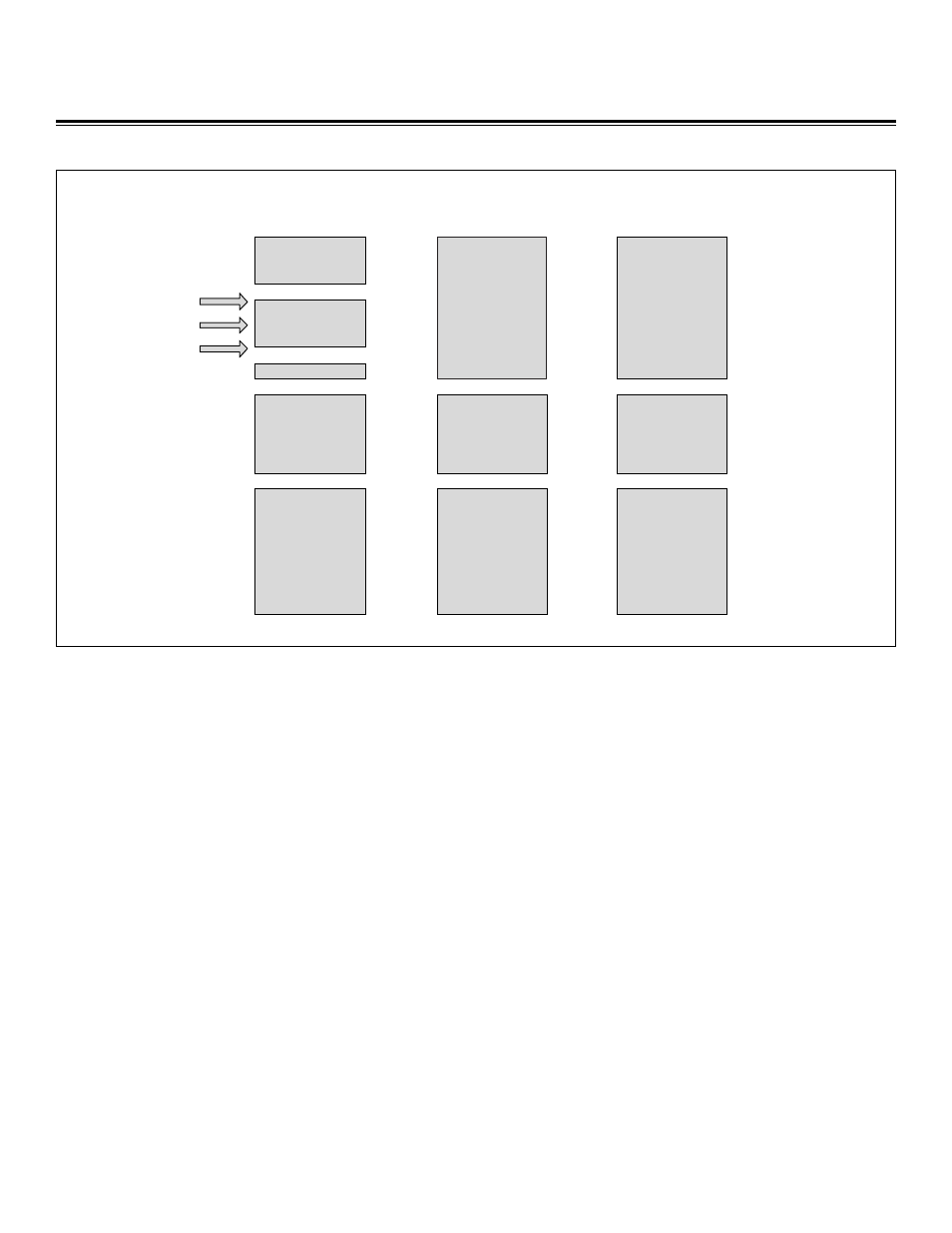
Figure 4: memory map when executing from data sram, Clock generation, Figure 4. memory map when executing from data sram – Maxim Integrated MAXQ Family Users Guide: MAXQ2000 Supplement User Manual
Page 11: Maxq family user’s guide: maxq2000 supplement
MAXQ Family User’s Guide:
MAXQ2000 Supplement
Clock Generation
All functional modules in the MAXQ2000 are synchronized to a single system clock. This system clock can be generated from one of
five possible sources (Figure 5):
• Internal ring oscillator
• Internal high-frequency oscillator using external crystal or resonator circuit
• External high-frequency clock signal
• Internal 32kHz oscillator using external crystal or resonator circuit
• External 32kHz clock signal
The MAXQ2000 does not provide the option for an external RC relaxation oscillator circuit.
Table 1 shows the registers and bits used to control clock generation and selection. For more information, see the register descriptions
in this guide and the MAXQ Family User’s Guide.
32k x 16
PROGRAM FLASH
OR MASKED ROM
PROGRAM
SPACE
EXECUTING FROM
DATA SPACE
(BYTE MODE)
DATA SPACE
(WORD MODE)
0000h
7FFFh
2k x 16
UTILITY ROM
87FFh
1k x 16
DATA SRAM
A000h
8000h
A3FFh
4k x 8
UTILITY ROM
8FFFh
8000h
64k x 8
PROGRAM FLASH
OR MASKED ROM
PAGE 0
(IF CDA0 = 0)
PAGE 1
(IF CDA0 = 1)
0000h
7FFFh
2k x 16
UTILITY ROM
87FFh
8000h
32k x 16
PROGRAM FLASH
OR MASKED ROM
PAGES 0 AND 1
0000h
7FFFh
Figure 4. Memory Map When Executing from Data SRAM
Maxim Integrated
11