Maxq family user’s guide: maxq2000 supplement – Maxim Integrated MAXQ Family Users Guide: MAXQ2000 Supplement User Manual
Page 22
MAXQ Family User’s Guide:
MAXQ2000 Supplement
The following section details the functionality of any System Registers contained in the MAXQ2000 that operate differently from their
descriptions in the MAXQ Family User’s Guide.
Register Name:
IMR
Register Description:
Interrupt Mask Register
Register Address:
AP[06h]
The first five bits in this register are interrupt mask bits for modules 0 through 4, one bit per module. The eighth bit, IMS, serves as a
mask for any system module interrupt sources. Setting a mask bit allows the enabled interrupt sources for the associated module or sys-
tem (with IMS) to generate interrupt requests. Clearing the mask bit effectively disables all interrupt sources associated with that mod-
ule or, in the case of IMS, all system interrupt sources. The IMR register is intended to facilitate user-definable interrupt prioritization.
Bit 0: (IMR.0) Module 0 Interrupt Mask (IM0)
Bit 1: (IMR.1) Module 1 Interrupt Mask (IM1)
Bit 2: (IMR.2) Module 2 Interrupt Mask (IM2)
Bit 3: (IMR.3) Module 3 Interrupt Mask (IM3)
Bit 4: (IMR.4) Module 4 Interrupt Mask (IM4)
Bits 5 and 6: (IMR.5 and IMR.6) Reserved
Bit 7: (IMR.7) System Module Interrupt Mask (IMS)
Register Name:
SC
Register Description:
System Control Register
Register Address:
AP[08h]
Bit 0: (SC.0) Reserved
Bit 1: (SC.1) Password Lock (PWL). This bit defaults to 1 on power-on reset only. When this bit is 1, it requires a 32-byte password
to be matched with the password in the program space before allowing access to the ROM Loader’s utilities for read/write of program
memory and debug functions. Clearing this bit to 0 disables the password protection to the ROM Loader.
Bits 2 and 3: (SC.2 and SC.3) Reserved
Bit 4: (SC.4) Code Data Access Bit 0 (CDA0). If this bit is set to 0, the lower half of physical program memory will be visible in data
space (when not executing from physical program memory) in byte mode. If this bit is set to 1, the upper half of physical program mem-
ory will be visible in data space in byte mode. When accessing data space in word mode, this bit has no effect.
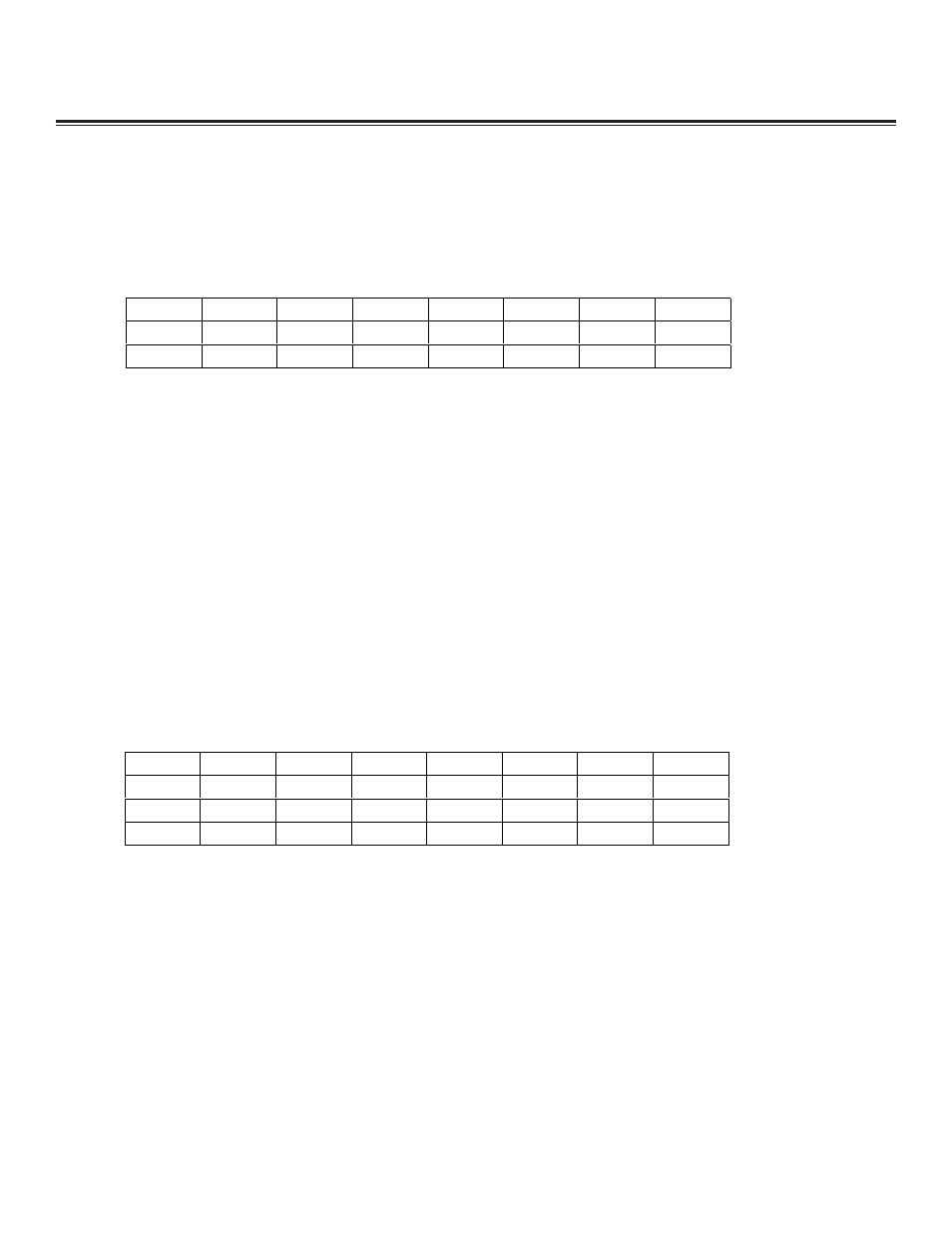
Bit #
7
6
5
4
3
2
1
0
Name
IMS
—
—
IM4
IM3
IM2
IM1
IM0
Reset
0
0
0
0
0
0
0
0
Access
r/w
r
r
r/w
r/w
r/w
r/w
r/w
Bit #
7
6
5
4
3
2
1
0
Name
TAP
—
—
CDA0
—
—
PWL
—
Reset
1
0
0
0
0
0
not set
0
POR
1
0
0
0
0
0
1
0
Access
r/w
r
r
r/w
r
r
r/w
r
Maxim Integrated
22