Addendum to section 3: programming, Table 4. system register map, Maxq family user’s guide: maxq2000 supplement – Maxim Integrated MAXQ Family Users Guide: MAXQ2000 Supplement User Manual
Page 19
Note that exiting Stop mode through external reset or power-on reset causes the processor to undergo a normal reset cycle, as
opposed to resuming execution at the point at which it entered Stop mode. Exiting Stop mode by means of an external interrupt or
time-of-day alarm causes the processor to resume execution at the instruction following the one that set the STOP bit.
When Stop mode is exited, processor execution resumes as follows.
• If the ring oscillator is selected as the system clock source (RGSL = 1), execution resumes using the ring oscillator as the system
clock following a delay of four ring cycles.
• If the high-frequency oscillator is selected as the system clock source (RGSL = 0), execution resumes using the ring oscillator as the
system clock following a delay of four ring cycles. After the high-frequency oscillator has completed its warmup period, the system
clock source switches over to the high-frequency clock automatically.
• If the 32kHz oscillator is selected as the system clock source, execution resumes using the 32kHz oscillator as the system clock fol-
lowing a delay of four ring cycles. For this to work properly, the 32kHz crystal amplifier must be enabled and running prior to enter-
ing Stop mode, or an external 32kHz clock must be provided immediately upon Stop mode exit (if X32D is set to 1).
ADDENDUM TO SECTION 3: PROGRAMMING
Refer to Section 3: Programming in the MAXQ Family User’s Guide for examples of general program operations involving the MAXQ
core. The MAXQ2000 contains the MAXQ20 (16-bit accumulator version) of the MAXQ core.
ADDENDUM TO SECTION 4: SYSTEM REGISTER DESCRIPTIONS
Refer to Section 4: System Register Descriptions in the MAXQ Family User’s Guide for functional descriptions of the registers and bits
listed in Tables 4, 5, and 6.
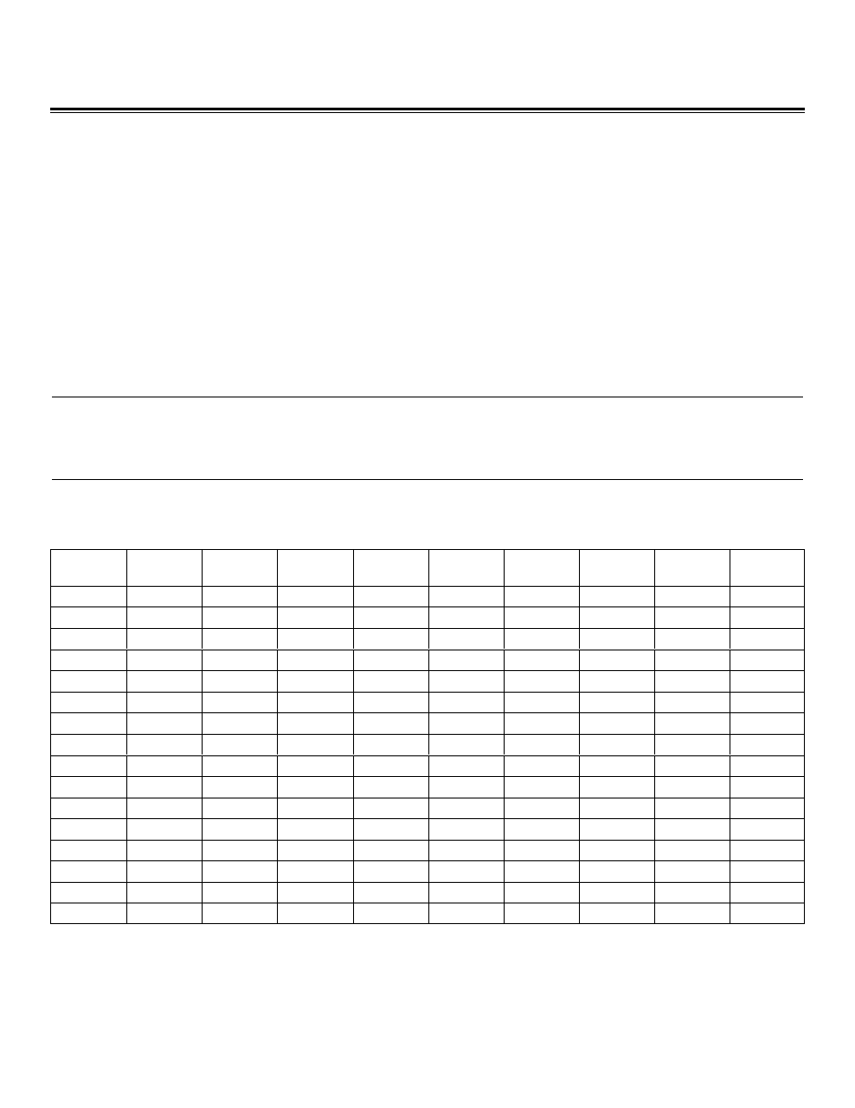
Table 4. System Register Map
Note: Register names that appear in italics indicate read-only registers. Register names that appear in bold indicate 16-bit registers. All other registers are 8
bits in width.
MAXQ Family User’s Guide:
MAXQ2000 Supplement
CYCLES TO
READ
CYCLES TO
WRITE
REGISTER
INDEX
AP (8h)
A (9h)
PFX (Bh)
IP (Ch)
SP (Dh)
DPC (Eh)
DP (Fh)
1
1
0xh
AP
A[0]
PFX
IP
1
1
1xh
APC
A[1]
SP
1
1
2xh
—
A[2]
IV
1
1
3xh
—
A[3]
Offs
DP[0]
1
1
4xh
PSF
A[4]
DPC
1
1
5xh
IC
A[5]
GR
1
1
6xh
IMR
A[6]
LC[0]
GRL
1
1
7xh
—
A[7]
LC[1]
BP
DP[1]
1
2
8xh
SC
A[8]
GRS
1
2
9xh
—
A[9]
GRH
1
2
Axh
—
A[10]
GRXL
1
2
Bxh
IIR
A[11]
FP
1
2
Cxh
—
A[12]
1
2
Dxh
—
A[13]
1
2
Exh
CKCN
A[14]
1
2
Fxh
WDCN
A[15]
Maxim Integrated
19