Sect. 15, Ripple attenuator module (ram / mi-ram) – Vicor VI-J00 Family DC-DC Converters and Configurable Power Supplies User Manual
Page 48

Design Guide & Applications Manual
For VI-200 and VI-J00 Family DC-DC Converters and Configurable Power Supplies
VI-200 and VI-J00 Family Design Guide
Rev 3.5
vicorpower.com
Page 47 of 98
Apps. Eng. 800 927.9474
800 735.6200
OVERVIEW
The RAM / MI-RAM is an accessory product for VI- / MI-200,
VI- / MI-J00, MegaMod /MI-MegaMod, ComPAC / MI-
ComPAC and FlatPAC. It reduces line frequency related
ripple and converter switching noise to less than 3 mV p-p
(10 mV p-p on the VI-J00).
Features include:
• Reduced differential noise (<3 mV p-p at loads up
to 20 A). The input of the RAM must be between
5 – 50 Vdc.
• Active and passive filtering
• Attenuation of low frequency input power source
harmonics and high frequency switching components
from DC-20 MHz
• Remote sense, trim, overvoltage protection and
overcurrent protection features retained
Applications for the RAM include medical diagnostic and
automated test equipment, radio receivers, transmitters
and communication products, and other products requiring
the noise performance of a linear supply. Refer to the
in Section 9.
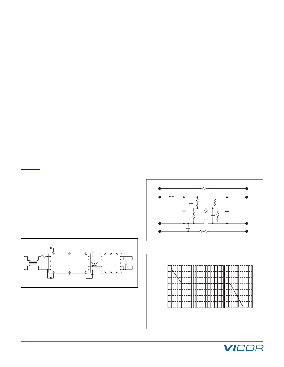
The RAM is a combination active / passive filter. A simplified
schematic is shown in Figure 15–2. The output of the
switcher feeds directly into a high frequency passive filter
which attenuates the switching noise. Low frequency, line
related ripple attenuation is via a FET series regulator that
maintains a constant average forward voltage drop of
about 350 mV. The FET gate is modulated to maintain the
AC component of the FET drain-source voltage equal to
the ripple component of the incoming DC voltage,
effectively cancelling it out.
The power supply’s sense leads feed through the RAM for
connection at the RAM output, for local sense, or at the
load, for remote sense (converter compensation is
0.5 V maximum). The attenuation and insertion loss are
constant up to 10 A or 20 A, depending on model. In
overload (above 10 A or 20 A), the voltage drop will
increase as the current increases. A single RAM can be
used on any output from 5 – 50 Vdc and will maintain the
original output setpoint of the converter within 0.5% at
the SENSE connection. Care should be taken not to
connect IN to OUT pins (i.e., through scope probe returns,
grounds, etc.) as attenuation will be adversely affected.
Inserting the RAM into the output leads of a Vicor
VI-200/VI-J00 converter adds phase shift to the converter’s
control loop. This occurs because voltage is sensed at the
output of the RAM’s internal filter. The 220µF capacitor
between –S IN and –IN (See Figure 15-1) provides additional
high frequency bypassing for the sense leads to ensure
stability of the converter and RAM. It may be possible to
reduce its value or remove it in applications where
transient response is important. If it is removed a network
analyzer should be used to verify stable operation.
15. Ripple Attenuator Module (RAM / MI-RAM)
VI- / MI-200
+OUT
–OUT
–S
+ S
+IN
–IN
TRIM
+
–
+IN
– IN
+OUT
–OUT
+S OUT
+ S IN
– S OUT
– S IN
N/C
RAM
Load
L1
GATE
IN
GATE
OUT
0.22 µF
220 µF
CM
Figure 15 –1 — RAM with optional trimming circuit and
recommended common-mode choke
60 db
55 db
25 db
30 db
35 db
40 db
45 db
50 db
10 MHz
1 MHz
100 KHz
10 KHz
1 KHz
100 Hz
10 Hz
Frequency
A
tt
e
n
u
a
ti
o
n
Figure 15 –3 — Attenuation vs. frequency (typical)
+S
+IN
–IN
–S
+S
+OUT
–OUT
–S
Figure 15 –2 — Basic RAM schematic
