Sect. 07, Figure 7–1) – Vicor VI-J00 Family DC-DC Converters and Configurable Power Supplies User Manual
Page 13

Design Guide & Applications Manual
For VI-200 and VI-J00 Family DC-DC Converters and Configurable Power Supplies
VI-200 and VI-J00 Family Design Guide
Rev 3.5
vicorpower.com
Page 12 of 98
Apps. Eng. 800 927.9474
800 735.6200
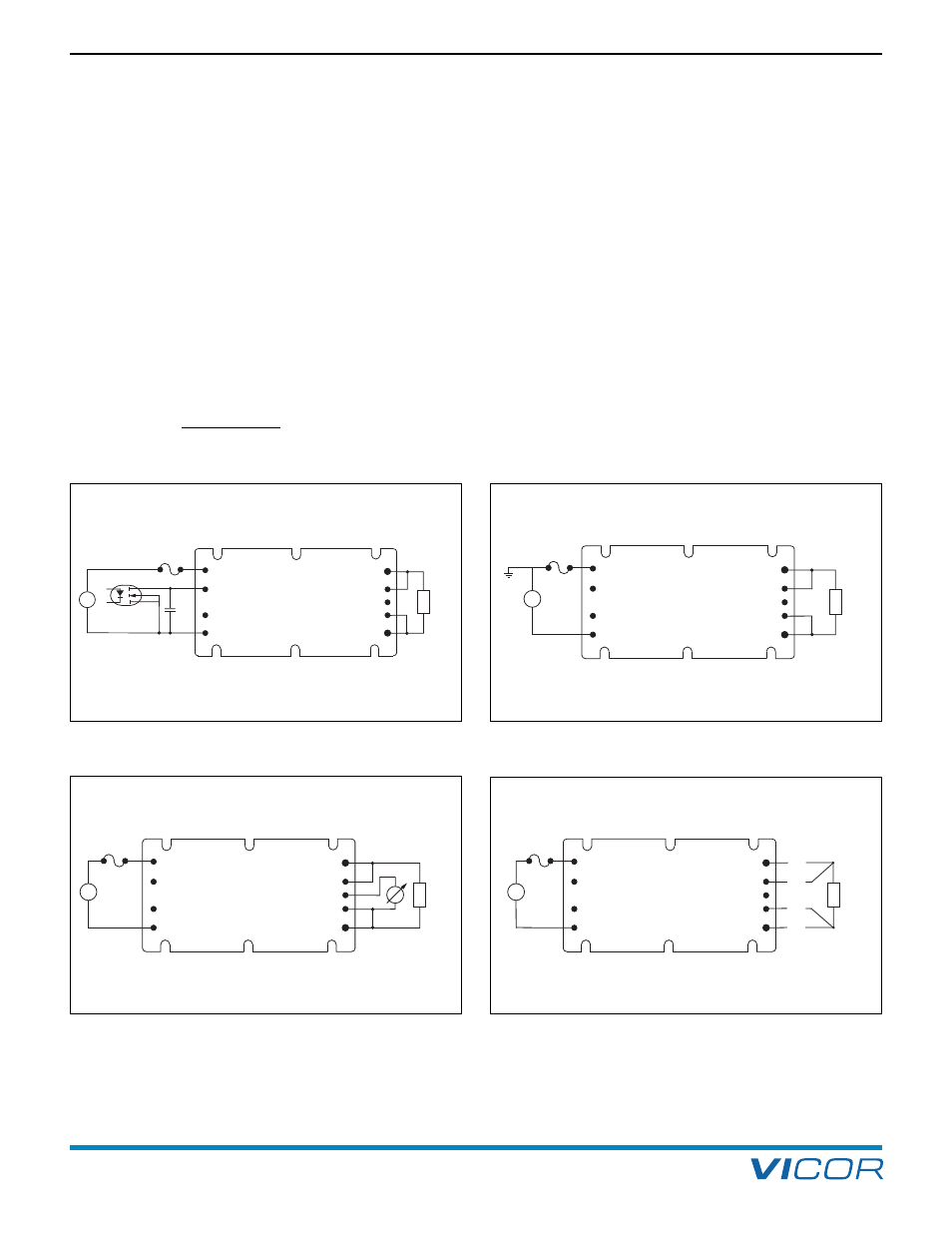
Logic Disable. (Figure 7–1) The GATE IN pin of the
module may be used to turn the module on or off. When
GATE IN is pulled low (<0.65 V @ 6 mA, referenced to
–Vin), the module is turned off. When GATE IN is floating
(open collector), the module is turned on. The open circuit
voltage of the GATE IN pin is less than 10 V. This applies
to VI-/ MI-200, VI-/ MI-J00 and MegaMod / MI-MegaMod
Family modules.
Output Voltage Programming. (Figure 7–2) Consult
Vicor’s Applications Engineering Department before
attempting large signal applications at high repetition
rates due to ripple current considerations with the internal
output capacitors. This applies to VI-/ MI-200, VI-/ MI-J00,
ComPAC / MI-ComPAC, FlatPAC and MegaMod /
MI-MegaMod Family modules.
V
out
=
Vtrim x Vnom
2.5
Negative Inputs (with positive ground). (Figure 7–3)
Vicor modules have isolated inputs and outputs making
negative input configurations easy. Fusing should always
be placed in the positive lead.
Remote Sensing. (Figure 7–4) Output voltage between
+OUT and –OUT must be maintained below 110% of
nominal. Do not exceed 0.25 V drop in negative return as
the current limit setpoint is moved out proportionately.
The sense should be closed at the module if remote
sensing is not desired. Applies to VI-/ MI-200, VI-/ MI-J00,
ComPAC / MI-ComPAC, FlatPAC and MegaMod /
MI-MegaMod Family modules. Excessively long sense leads
and / or excessive external capacitance at the load may
result in module instability. Please consult Vicor
Applications Engineering for compensation methods.
–OUT
–S
+S
+OUT
+IN
GATE
IN
GATE
OUT
–IN
Zero Current
Switching
Converter
Driver
+
–
1
6
TLP798G
Agilent 6N139
Load
2
5
TRIM
1µF
7. Application Circuits / Converter Array Design Considerations
Figure 7–1 — Logic disable
Figure 7–2 — Output voltage programming
–OUT
–S
TRIM
+S
+OUT
+IN
GATE
IN
GATE
OUT
–IN
Zero Current
Switching
Converter
Driver
+
–
Load
Figure 7–3 — Negative inputs (with positive ground)
–OUT
–S
TRIM
+S
+OUT
+IN
GATE
IN
GATE
OUT
–IN
Zero Current
Switching
Converter
Driver
+
–
Load
• • •
• • •
• • •
• • •
• • •
• • •
• • •
• • •
Figure 7–4 — Remote sensing
