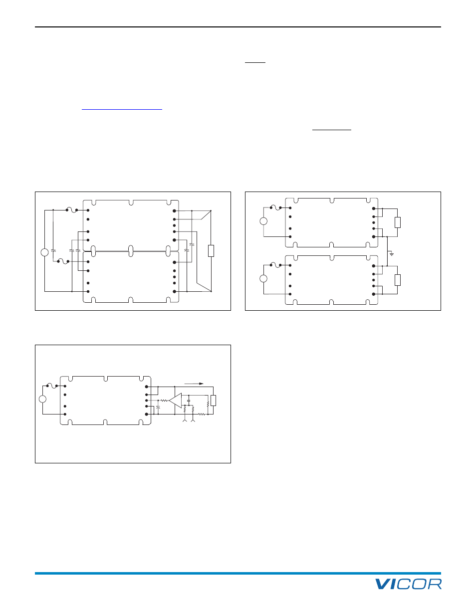
Figure 7–5), Figure 7–6 — programmable current source, Figure 7–7 — dual output voltages – Vicor VI-J00 Family DC-DC Converters and Configurable Power Supplies User Manual
Page 14

Design Guide & Applications Manual
For VI-200 and VI-J00 Family DC-DC Converters and Configurable Power Supplies
VI-200 and VI-J00 Family Design Guide
Rev 3.5
vicorpower.com
Page 13 of 98
Apps. Eng. 800 927.9474
800 735.6200
Parallel Boost. (Figure 7–5) U.S. Patent #4,648,020 —
other patents pending. To retain accurate power sharing
between a Driver and (n) number of Boosters, provide
adequate input and output power bussing. This applies to
VI-/ MI-200 and MegaMod / MI-MegaMod Family
modules. See
for recommended
external components. (Section 3)
Programmable Current Source. (Figure 7–6) Module
output voltage should not exceed the rated voltage of the
operational amplifier. This applies to VI-/ MI-200,
VI-/ MI-J00, ComPAC / MI-ComPAC, FlatPAC and
MegaMod / MI-MegaMod Family modules.
NOTE: When using a VI-J00 module, the TRIM pin
voltage should be clamped to 2.75 V to avoid
damage to the module. This corresponds to the
maximum trim up voltage. This circuit or functional
equivalent must be used when charging batteries.
Do not exceed the nominal current ratings of the
converter. Example,
Pout
Vnominal
Dual Output Voltages. (Figure 7–7) Vicor modules have
isolated outputs so they can easily be referenced to a
common node creating positive and / or negative rails.
7. Application Circuits / Converter Array Design Considerations
Figure 7–5 — Parallel boost. U.S. Patent #4,648,020 — other
patents pending.
–OUT
–S
TRIM
+S
+OUT
+IN
GATE
IN
GATE
OUT
–IN
Zero Current
Switching
Converter
#1
Driver
VI-2xx-xx
+
–
–OUT
–S
TRIM
+S
+OUT
+IN
GATE
IN
GATE
OUT
–IN
Zero Current
Switching
Converter
#n
Booster
VI-Bxx-xx
Load
Figure 7–6 — Programmable current source
–OUT
-S
TRIM
+S
+OUT
+IN
GATE
IN
GATE
OUT
–IN
Zero Current
Switching
Converter
Driver
+
–
Load
V Control
0.1 V/A
1K
OP
AMP
–
+
1K 1K
0.05
Ω
1K
0.01
I
10 µF
–OUT
–S
TRIM
+S
+OUT
+IN
GATE
IN
GATE
OUT
–IN
Zero Current
Switching
Converter
Driver
+
–
Load requiring
positive output
–OUT
–S
TRIM
+S
+OUT
+IN
GATE
IN
GATE
OUT
–IN
Zero Current
Switching
Converter
Driver
+
–
Load requiring
negative output
Figure 7–7 — Dual output voltages
