Sect. 01, Zero-current-switching – Vicor VI-J00 Family DC-DC Converters and Configurable Power Supplies User Manual
Page 3
Design Guide & Applications Manual
For VI-200 and VI-J00 Family DC-DC Converters and Configurable Power Supplies
VI-200 and VI-J00 Family Design Guide
Rev 3.5
vicorpower.com
Page 2 of 98
Apps. Eng. 800 927.9474
800 735.6200
OVERVIEW
Vicor offers RoHS compliant modules. These modules have
a “VE” prefix. The information presented herein applies to
both versions, and “VI” will be the default designation.
The heart of Vicor’s VI-/ MI-200 and VI-/ MI-J00 module
technology, zero-current-switching, allows Vicor
converters to operate at frequencies in excess of 1 MHz,
with high efficiency and power density. Depending on
input voltage and load, the converters operate at
frequencies ranging from the low hundreds of kilohertz
(light load, high line) to approximately one megahertz (full
load, low line). Another aspect of the Vicor topology is
that two or more power trains driven at the same
frequency will inherently load-share if their outputs are
tied together. Load sharing is dynamic and is within 5%.
The VI-200 and MI-200 product line offer both Driver and
Booster modules:
• Drivers and Boosters must have identical power trains.
• Drivers close the voltage loop internally, Boosters do not.
• Boosters may be slaved to a Driver, allowing
configurations of multi-kilowatt arrays, which
exhibit dynamic current sharing between modules.
• Only a single control connection is needed between
modules with all module’s power inputs and outputs,
connected together — no trimming, adjustments, or
external components are required to achieve load sharing.
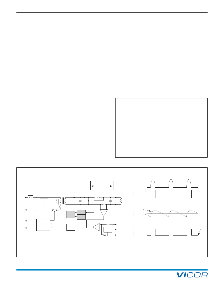
LOSSLESS ENERGY TRANSFER
Referring to Figure and Table 1–1 below, turn-on of the
MOSFET switch transfers a quantized energy packet from
the input source to an LC “tank” circuit, composed of
inherent transformer leakage inductance of T1 and a
capacitive element, C, in the secondary. Simultaneously,
an approximately half-sinusoidal current flows through the
switch, resulting in switch turn-on at zero current and
turn-off when current returns to zero. Resonance, or
bidirectional energy flow, cannot occur because D1 will
only permit unidirectional energy transfer. A low-pass filter
(Lo, Co) following the capacitor produces a low ripple DC
output. The result is a virtually lossless energy transfer
from input to output with greatly reduced levels of
conducted and radiated noise.
Ip: Primary current
Vp: Primary voltage
Vs: Secondary voltage
OVP: Overvoltage protection (output)
OTS: Over temperature shutdown
OC1, OC2: Opto-coupler
E/A: Error amplifier
REF: Bandgap reference
C/L: Current limit amplifier
Referenced
to –Vin
[a]
Not in VI-J00 Series
Gate
Out
Vs
Vout
Vin
Ip
Vp
2.5 V
REF.
Output Filter
Integrator
Vs
Ip
Vp
MOSFET
Input
Filter
OC2
OC1
[a]
–S
TRIM
+S
E/A
+
+
–
+Vout
–Vout
Co
Lo
C
D2
D1
Reset
Control
GATE
IN
-Vin
+Vin
Logic
Control
Load
C/L
OTS
[a]
OVP
[a]
GATE
OUT
–
T1
1. Zero-Current-Switching
Figure 1–1 — VI- /MI-200 and VI- /MI-J00 series zero-current-switching block diagram
Table 1–1