External space, Section “external space, At8xc51snd1c – Rainbow Electronics AT89C51SND1C User Manual
Page 25
25
AT8xC51SND1C
4109E–8051–06/03
External Space
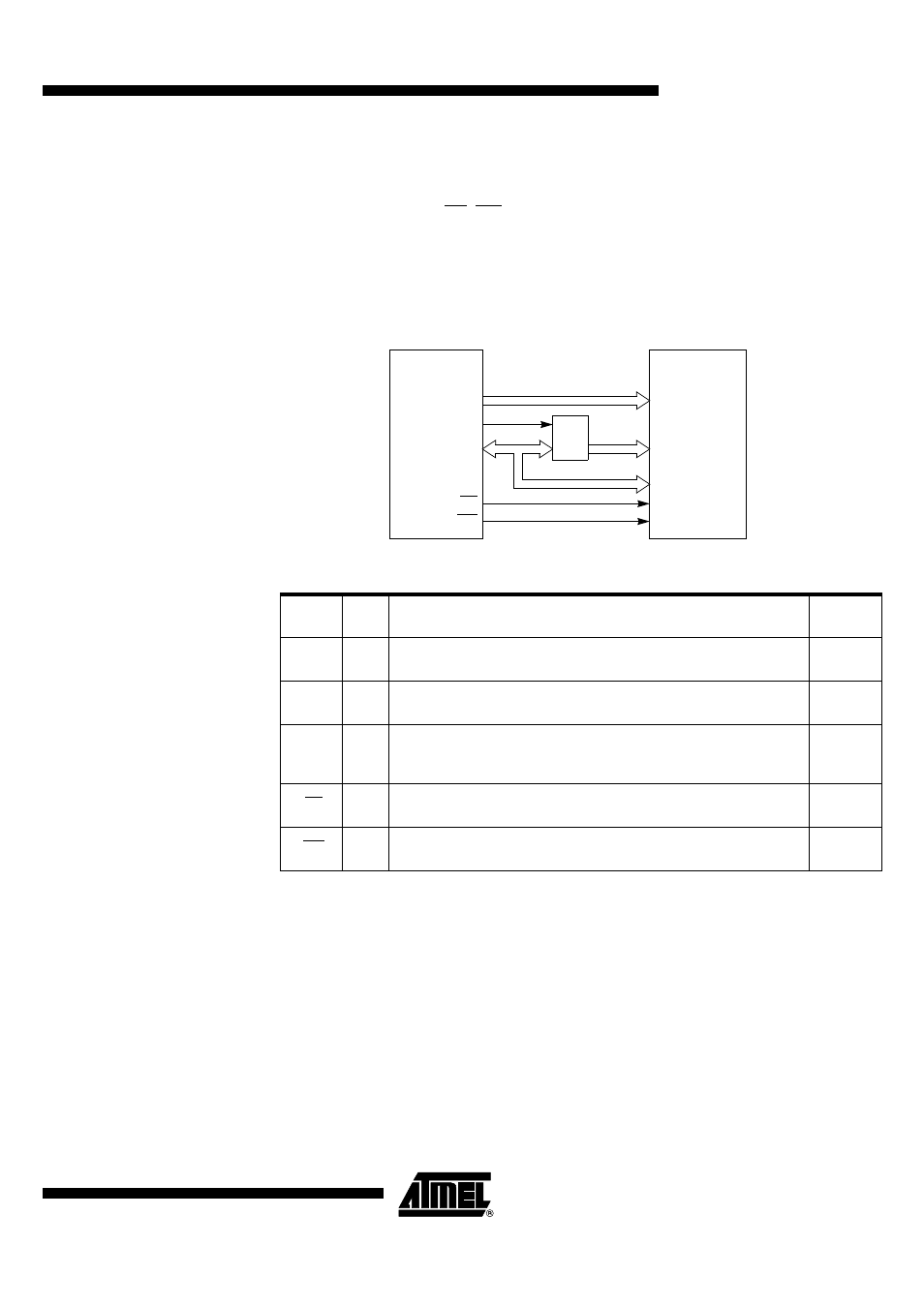
Memory Interface
The external memory interface comprises the external bus (port 0 and port 2) as well as
the bus control signals (RD, WR, and ALE).
Figure 17 shows the structure of the external address bus. P0 carries address A7:0
while P2 carries address A15:8. Data D7:0 is multiplexed with A7:0 on P0. Table 27
describes the external memory interface signals.
Figure 17. External Data Memory Interface Structure
Table 27. External Data Memory Interface Signals
Page Access Mode
The AT8xC51SND1C implement a feature called Page Access that disables the output
of DPH on P2 when executing MOVX @DPTR instruction. Page Access is enable by
setting the DPHDIS bit in AUXR register.
Page Access is useful when application uses both ERAM and 256 Bytes of XRAM. In
this case, software modifies intensively EXTRAM bit to select access to ERAM or XRAM
and must save it if used in interrupt service routine. Page Access allows external access
above 00FFh address without generating DPH on P2. Thus ERAM is accessed using
MOVX @Ri or MOVX @DPTR with DPTR < 0100h, and XRAM is accessed using
MOVX @DPTR with DPTR
≥
0100h while keeping P2 for general I/O usage.
Signal
Name
Type
Description
Alternate
Function
A15:8
O
Address Lines
Upper address lines for the external bus.
P2.7:0
AD7:0
I/O
Address/Data Lines
Multiplexed lower address lines and data for the external memory.
P0.7:0
ALE
O
Address Latch Enable
ALE signals indicates that valid address information are available on lines
AD7:0.
-
RD
O
Read
Read signal output to external data memory.
P3.7
WR
O
Write
Write signal output to external memory.
P3.6
RAM
PERIPHERAL
AT8xC51SND1C
P2
P0
AD7:0
A15:8
A7:0
A15:8
D7:0
A7:0
ALE
WR
OE
RD
WR
Latch