Registers, Table 147), Table 148) – Rainbow Electronics AT89C51SND1C User Manual
Page 177: At8xc51snd1c
177
AT8xC51SND1C
4109E–8051–06/03
Registers
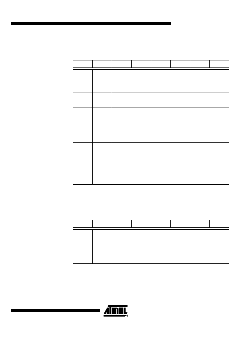
Table 147. ADCON Register
ADCON (S:F3h) – ADC Control Register
Reset Value = 0000 0000b
Table 148. ADCLK Register
ADCLK (S:F2h) – ADC Clock Divider Register
Reset Value = 0000 0000b
7
6
5
4
3
2
1
0
-
ADIDL
ADEN
ADEOC
ADSST
-
-
ADCS
Bit
Number
Bit
Mnemonic
Description
7
-
Reserved
The value read from this bit is always 0. Do not set this bit.
6
ADIDL
ADC Pseudo-Idle Mode
Set to suspend the CPU core activity (pseudo-idle mode) during conversion.
Clear by hardware at the end of conversion.
5
ADEN
ADC Enable Bit
Set to enable the A to D converter.
Clear to disable the A to D converter and put it in low power stand by mode.
4
ADEOC
End Of Conversion Flag
Set by hardware when ADC result is ready to be read. This flag can generate an
interrupt.
Must be cleared by software.
3
ADSST
Start and Status Bit
Set to start an A to D conversion on the selected channel.
Cleared by hardware at the end of conversion.
2 - 1
-
Reserved
The value read from these bits is always 0. Do not set these bits.
0
ADCS
Channel Selection Bit
Set to select channel 0 for conversion.
Clear to select channel 1 for conversion.
7
6
5
4
3
2
1
0
-
-
-
ADCD4
ADCD3
ADCD2
ADCD1
ADCD0
Bit
Number
Bit
Mnemonic
Description
7 - 5
-
Reserved
The value read from these bits is always 0. Do not set these bits.
4 - 0
ADCD4:0
ADC Clock Divider
5-bit divider for ADC clock generation.