At8xc51snd1c, 7 to 3.3 v, t, 40 to +85 ° c – Rainbow Electronics AT89C51SND1C User Manual
Page 194: Waveforms figure 150. two wire waveforms
194
AT8xC51SND1C
4109E–8051–06/03
Two-wire Interface
Timings
Table 167. TWI Interface AC Timing
V
DD
= 2.7 to 3.3 V, T
A
= -40 to +85
°
C
Notes:
1. At 100 kbit/s. At other bit-rates this value is inversely proportional to the bit-rate of
100 kbit/s.
2. Determined by the external bus-line capacitance and the external bus-line pull-up
resistor, this must be < 1
µ
s.
3. Spikes on the SDA and SCL lines with a duration of less than 3·T
CLCL
will be filtered
out. Maximum capacitance on bus-lines SDA and
SCL= 400 pF.
4. T
CLCL
= T
OSC
= one oscillator clock period.
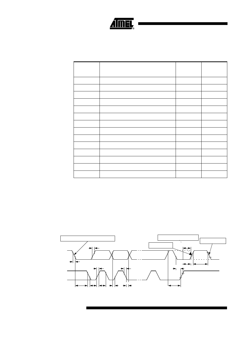
Waveforms
Figure 150. Two Wire Waveforms
Symbol
Parameter
INPUT
Min
Max
OUTPUT
Min
Max
T
HD
; STA
Start condition hold time
14·T
CLCL
(4)
4.0
µ
s
(1)
T
LOW
SCL low time
16·T
CLCL
(4)
4.7
µ
s
(1)
T
HIGH
SCL high time
14·T
CLCL
(4)
4.0
µ
s
(1)
T
RC
SCL rise time
1
µ
s
-
(2)
T
FC
SCL fall time
0.3
µ
s
0.3
µ
s
(3)
T
SU
; DAT1
Data set-up time
250 ns
20·T
CLCL
(4)
- T
RD
T
SU
; DAT2
SDA set-up time (before repeated START condition)
250 ns
1
µ
s
(1)
T
SU
; DAT3
SDA set-up time (before STOP condition)
250 ns
8·T
CLCL
(4)
T
HD
; DAT
Data hold time
0 ns
8·T
CLCL
(4)
- T
FC
T
SU
; STA
Repeated START set-up time
14·T
CLCL
(4)
4.7
µ
s
(1)
T
SU
; STO
STOP condition set-up time
14·T
CLCL
(4)
4.0
µ
s
(1)
T
BUF
Bus free time
14·T
CLCL
(4)
4.7
µ
s
(1)
T
RD
SDA rise time
1
µ
s
-
(2)
T
FD
SDA fall time
0.3
µ
s
0.3
µ
s
(3)
Tsu;DAT1
T
su
;STA
Tsu;DAT
2
T
hd
;STA
T
high
T
low
SDA
(INPUT/OUTPUT)
0.3 V
DD
0.7 V
DD
T
buf
T
su
;STO
0.7
V
DD
0.3 V
DD
T
rd
T
fd
T
rc
T
fc
SCL
(INPUT/OUTPUT)
T
hd;
DAT
T
su;
DAT3
START or Repeated START condition
START condition
STOP condition
Repeated START condition